The technique was reported in Nature Communications by researchers from KTH Royal Institute of Technology in Stockholm, in collaboration with RWTH Aachen University, Universität der Bundeswehr München, AMO GmbH and Protemics GmbH, in Germany.
A reliable, industrially-scalable method of integrating 2D materials, such as graphene, with silicon semiconductors would help downscale electronics and usher in new capabilities for sensor technology and photonics.
However, the integration of 2D material to the semiconductor, or a substrate with integrated electronics, is fraught with a number of challenges.
“There’s always this critical step of transferring from a special growth substrate to the final substrate on which you build sensors or components,” says Arne Quellmalz, a researcher in photonic microsystems at KTH.
“You might want to combine a graphene photodetector for optical on-chip communication with silicon read-out electronics,” Quellmalz says. “But the growth temperatures of those materials is too high, so you cannot do this directly on the device substrate.”
Experimental methods for transferring grown 2D material to desired electronics have been beset by a number of deficiencies, such as degradation of the material and its electronic transport properties, or by contamination of the material.
Quellmalz says that the solution lies in the existing toolkits of semiconductor manufacturing: to use a standard dielectric material called bisbenzocyclobutene (BCB), along with conventional wafer bonding equipment.
“We basically glue the two wafers together with a resin made of BCB,” he says. “We heat the resin, until it becomes viscous, like honey, and press the 2D material against it.”
At room temperature, the resin becomes solid and forms a stable connection between the 2D material and the wafer, he says. “To stack materials, we repeat the steps of heating and pressing. The resin becomes viscous again and behaves like a cushion, or a waterbed, which supports the layer stack and adapts to the surface of the new 2D material.”
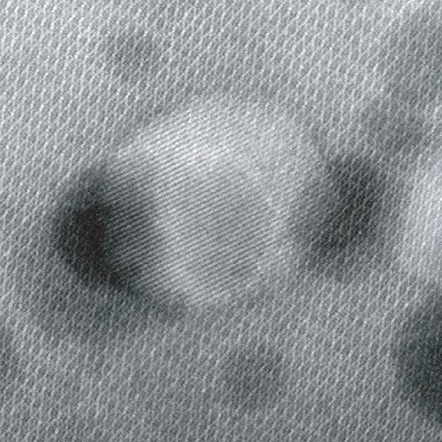
The researchers demonstrated the transfer of graphene and molybdenum disulfide (MoS2), as a representative for transition metal dichalcogenides, and stacked graphene with hexagonal boron nitride (hBN) and MoS2 to heterostructures. All transferred layers and heterostructures were reportedly of high quality, that is, they featured uniform coverage over up to 100-millimeter sized silicon wafers and exhibited little strain in the transferred 2D materials, the paper states.
Read the original article on KTH Royal Institute of Technology.