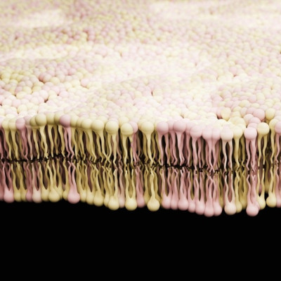
This new design is based on a “metasurface”, in other words a surface made up of small structures that are repeated in a pattern. In addition to this, both the structures and the pattern are smaller than the wavelength of light. This means that they need to be nanometric in size (millionths of a millimetre), explain researchers from the UC3M’s Displays and Photonic Applications Group (GDAF, in its Spanish acronym). This is a surface made up of small structures that are repeated in a pattern. In addition to this, both the structures and the pattern are smaller than the wavelength of light.
The design they have suggested is to emboss crosses on a hydrogenated amorphous thin-layer silicon solar cell, specifically, on the transparent conductive layer where the light enters. Then, dielectric material nanospheres fill these crosses. By doing so, the light that reaches the cell is effectively redirected to its active area, the place where it is transformed into an electric current by the photoelectric effect. Using this technique, more light can be captured in the solar cell, generating up to 40% more of generated current, according to their calculations, which have been published in a paper in the Solar Energy journal.
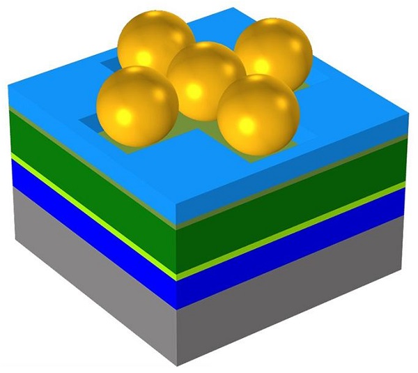
The pattern proposed by researchers is based on zinc oxide spheres with a radius of 210 nanometres deposited over crosses on thin-layer silicon solar cells.
In this work, researchers have been able to determine the correct material for the nanospheres, such as zinc oxide, as well as the correct size so that it’s possible to manufacture them currently: a radius of 210 nanometres (the thickness of a human hair ranges from 60,000 to 80,000 nanometres).
“The key to achieving this effectively in certain “colours” is choosing the correct sizes and materials”, explains one of the study’s authors, Ricardo Vergaz, lecturer at the UC3M’s Department of Electronic Technology. “We have evaluated thousands of possible sizes and refractive indices, the most important optical property of the spheres’ material”, he adds.
The strategy: combine diffraction and resonant effects
Embedding the spheres into the crosses, and therefore, bringing them slightly closer to the active layer below, increases their effect greatly, the researchers highlight in the study. In addition to this, they have found that the combination of the effect of the crosses and spheres is what causes this improvement. If the crosses are separated, or the spheres are reduced, the effect declines dramatically.
“We have tried to enhance the diffraction produced by the crosses by the resonant effects of the spheres themselves,” notes another of the study’s authors, Braulio García-Camara, a researcher at the GDAF. “The contrasts between the refraction indices of the nanospheres and those on the lower layers allow us to exploit the effects we were looking for. Once this design can be implemented into manufacturing, a significant improvement in performance will be achieved in solar cells installed in future solar fields,” he concludes.
Another advantage of this design is that the effects produced allow the thickness of the active layer to be reduced in order to generate the current efficiently, saving material during the manufacturing process. “By reducing this, the extraction of electrons generated by light is also more effective, as they have less path to cross where they could be reabsorbed”, they highlight. In addition to this, the absorption that occurs in the layers surrounding the active layer has a warming effect, which can allow its defects to be reduced in the long term.
Read the original article on Universidad Carlos III de Madrid (UC3M).


