

Rare-earth nickelate oxides, also called nickelates, have attracted a lot of interest from researchers because they display an electronic phase transition, which may be exploited in future electronic devices. This particular phase transition consists of turning from a metallic state that conducts electricity into an electrically-insulating state as temperature drops.
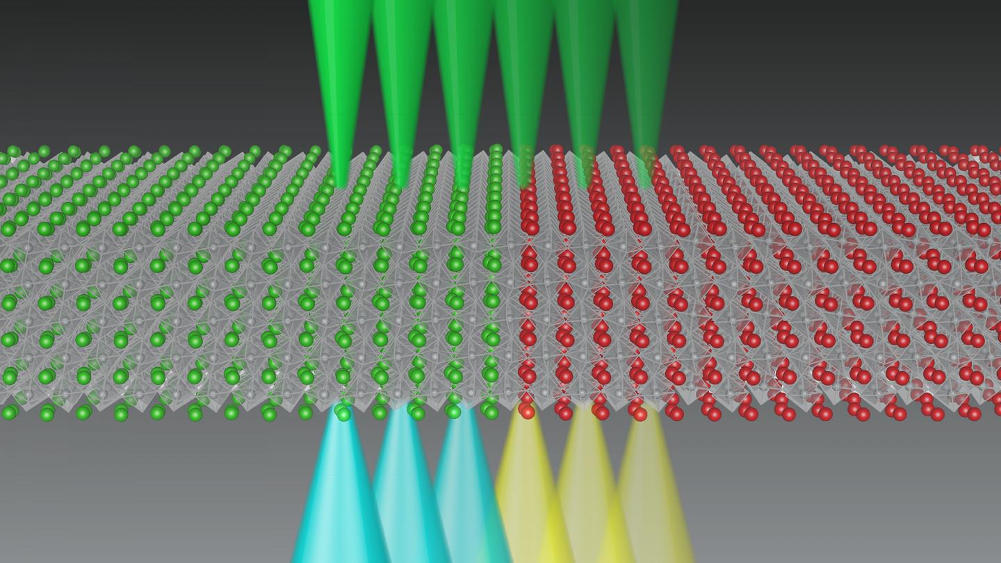
Schematic illustration of a STEM probe scanning across the interface of two nickelate compounds, with the nature of the scattered electrons changing as the electronic phase of the material goes from being metallic to insulating. Atomic structure model rendered using VESTA.
Behind this behaviour is a strong interaction between the electronic properties of these compounds and their "lattice" structure - the well-ordered arrangement of atoms that forms a crystal. However, uncovering the true nature of this metal to insulator phase transition in nickelates, and being able to control it for potential electronic devices, requires knowing how each characteristic phase emerges and evolves across the transition.
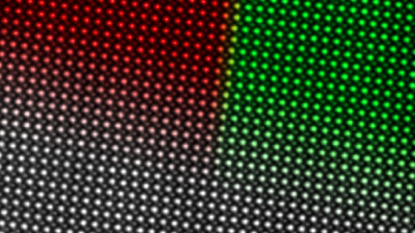
Atomic resolution STEM image showing the perfect crystal structure of a nickelate thin film, coloured to represent the two compounds.
Now, scientists from EPFL and the University of Geneva have combined two cutting-edge techniques to achieve nanoscale mapping of each distinct electronic phase. Published in the journal Nano Letters, the study was led by Dr Duncan Alexander at EPFL's School of Basic Sciences and the group of Professor Jean-Marc Triscone at the University of Geneva.
The study's first author, Dr Bernat Mundet, says: "To fully understand the physics displayed by novel electronic materials and to control them in devices, new atomic-scale characterization techniques are required. In this regard, we have been able for the first time to precisely determine the metallic and insulating regions of atomically engineered devices made from two nickelate compounds with near atomic resolution. We believe that our methodology will help to better understand the physics of this important family of electronic materials."
The researchers combined aberration-corrected scanning transmission electron microscopy (STEM) with monochromated electron energy-loss spectroscopy (EELS).
In STEM, images are formed by scanning a beam of electrons, focused to a spot of about 1 Ångstroms in size, across a sufficiently thin specimen - in this case a sliver of nickelate - and collecting the transmitted and scattered electrons with the use of annular detectors. Though technically demanding, this technique allows researchers to precisely visualise a crystal's lattice structure, atomic row by atomic row.
For the second technique, EELS, those electrons passing through the central hole of the annular detector are instead collected. Some of these electrons have previously lost some energy due to their interaction with the Ni atoms of the nickelate crystal. By measuring how this energy difference changes, we can determine the metallic or insulating state of the nickelate compound.
Since all electrons are scattered and collected simultaneously, the researchers were able to correlate the electronic state changes with the associated lattice positions in the different nickelate compounds. This approach allowed them to map, for the first time, the spatial configuration of their metallic or insulating regions, reaching a very high spatial resolution of around 3.5 Ångstroms (0.35 nanometers). The technique will be a valuable tool for studying and guiding the atomic engineering of these novel electronic materials.
"The latest electron microscopes give us an amazing ability to measure a variety of materials physical properties with atomic or nanometric spatial resolution," says Duncan Alexander. "Here, by pushing the capabilities of EPFL's Titan Themis microscope to the limits, we take an exciting step forward in this domain, by proving that we can measure the changes in electronic state across a thin film structure precisely made from two different nickelates. Our approach opens up new avenues for investigating the physics of these nickelate compounds, which have sparked research interest worldwide."
"The combination of amazing artificial materials that display a metal to insulator transition and very advanced electron microscopy has allowed unprecedented detailed investigations of their electronic properties," adds Jean-Marc Triscone. "In particular, it revealed, at the atomic scale, whether the material is conducting or insulating - an important question for better understanding these materials that may be used in future computing approaches."
Read the original article on EurekAlert.
