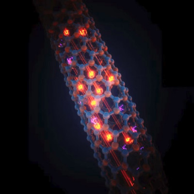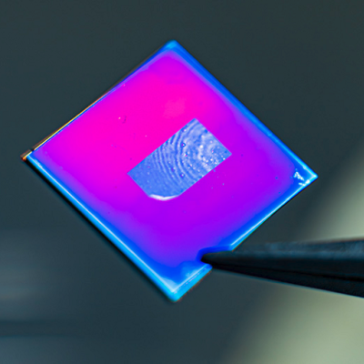
A Rice University laboratory has adapted its laser-induced graphene technique to make high-resolution, micron-scale patterns of the conductive material for consumer electronics and other applications.
Laser-induced graphene (LIG), introduced in 2014 by Rice chemist James Tour, involves burning away everything that isn’t carbon from polymers or other materials, leaving the carbon atoms to reconfigure themselves into films of characteristic hexagonal graphene.
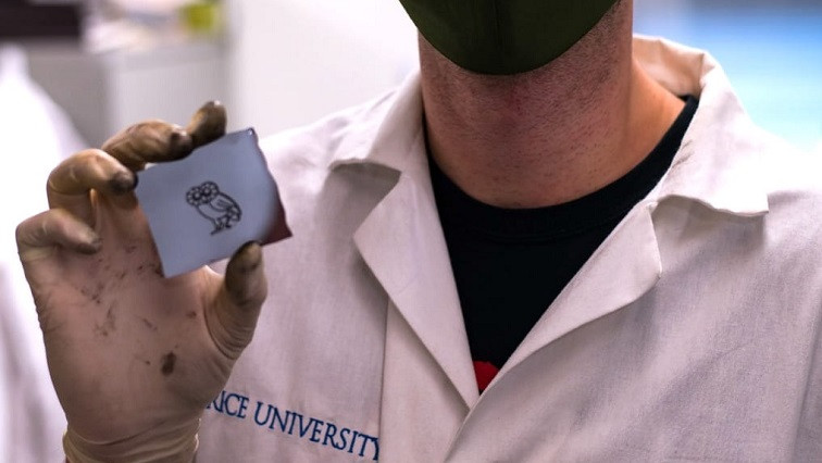
The process employs a commercial laser that “writes” graphene patterns into surfaces that to date have included wood, paper and even food.
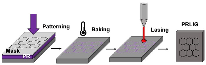
The new iteration writes fine patterns of graphene into photoresist polymers, light-sensitive materials used in photolithography and photoengraving. Baking the film increases its carbon content, and subsequent lasing solidifies the robust graphene pattern, after which unlased photoresist is washed away.
Details of the PR-LIG process appear in the American Chemical Society journal ACS Nano.
“This process permits the use of graphene wires and devices in a more conventional silicon-like process technology,” Tour said. “It should allow a transition into mainline electronics platforms.”
The Rice lab produced lines of LIG about 10 microns wide and hundreds of nanometers thick, comparable to that now achieved by more cumbersome processes that involve lasers attached to scanning electron microscopes, according to the researchers.
Rice University chemists have adapted their laser-induced graphene process to make conductive patterns from standard photoresist material for consumer electronics and other applications.
Achieving lines of LIG small enough for circuitry prompted the lab to optimize its process, according to graduate student Jacob Beckham, lead author of the paper.
“The breakthrough was a careful control of the process parameters,” Beckham said. “Small lines of photoresist absorb laser light depending on their geometry and thickness, so optimizing the laser power and other parameters allowed us to get good conversion at very high resolution.”
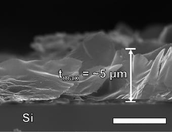
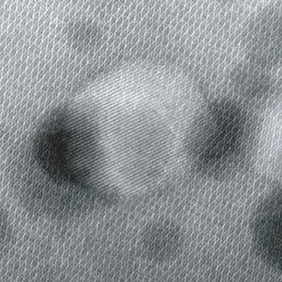
A scanning electron microscope image shows a cross-section of laser-induced graphene on silicon. The graphene was created at Rice University by lasing a photoresist polymer to make micron-scale lines that could be useful for electronics and other applications. The scale bar is 5 microns.
Because the positive photoresist is a liquid before being spun onto a substrate for lasing, it’s a simple matter to dope the raw material with metals or other additives to customize it for applications, Tour said.
Potential applications include on-chip microsupercapacitors, functional nanocomposites and microfluidic arrays.
Read the original article on Rice University.