Recently, Professor Jiang Ying from International Center for Quantum Materials and Research Center for Light-Element Advanced Materials of Peking University, in collaboration with Professor Jörg Wrachtrup from Stuttgart University and Professor Yang Sen from the Chinese University of Hong Kong, has developed a scanning quantum sensing microscope by using a solid-state quantum bit (qubit), nitrogen-vacancy (NV) center, as the quantum sensor. They have, for the first time, realized NV-based nanoscale electric-field imaging and its charge-state control, demonstrating the possibility of scanning NV electrometry. This work, titled “Nanoscale electric-field imaging based on a quantum sensor and its charge-state control under ambient condition”, has been published in Nature Communications 12, 2457 (2021).
Nitrogen-vacancy (NV) center is a point defect hosted in the diamond, which is regarded as one of the most promising solid-state qubit for quantum computation, quantum information and quantum sensing. The NV has been applied as a powerful quantum sensor for detecting subtle magnetic/electric signals in a quantitative manner, based on monitoring the coherent evolution of its quantum state during its interaction with the surrounding environment. Since the NV has long coherence time up to ~ms even under ambient condition, the sensitivity of NV is exceptionally high, even allowing to detect single nuclear/electron spin. By integrating the shallow NV with scanning probe microscope (SPM), one can construct scanning magnetometry and realize quantitative magnetic imaging at nanoscale. However, the nanoscale electric-field mapping has not been achieved so far because of the relatively weak coupling strength between NV and the electric field, leading to the stringent requirements on both the coherence of shallow NV and the stability of SPM system.
Professor Jiang Ying and his group have been for a long time devoted to the development of advanced SPM systems. Recently, they have developed a new-generation qPlus-based atomic force microscope (AFM), which pushes the resolution and sensitivity of SPM to the classical limit and allows the direct imaging of hydrogen atom in water molecules. On this basis, this group integrated the NV-based quantum sensing technology into a qPlus-based SPM system, resulting in the so-called scanning quantum sensing microscope. Due to the ultrahigh stability of qPlus sensor, it can work with very small amplitude (~100 pm) at a close tip-surface distance of ~1 nm, which is critical to maintain the good coherence and resolution of shallow NV. Using the single shallow NV, the team was able to map the local electric field from a biased metal tip with a spatial resolution of ~10 nm and a sensitivity close to an elementary charge. In the future, this technique can be applied for investigating the local charge, polarization and dielectric response of the functional materials from a microscopic view.
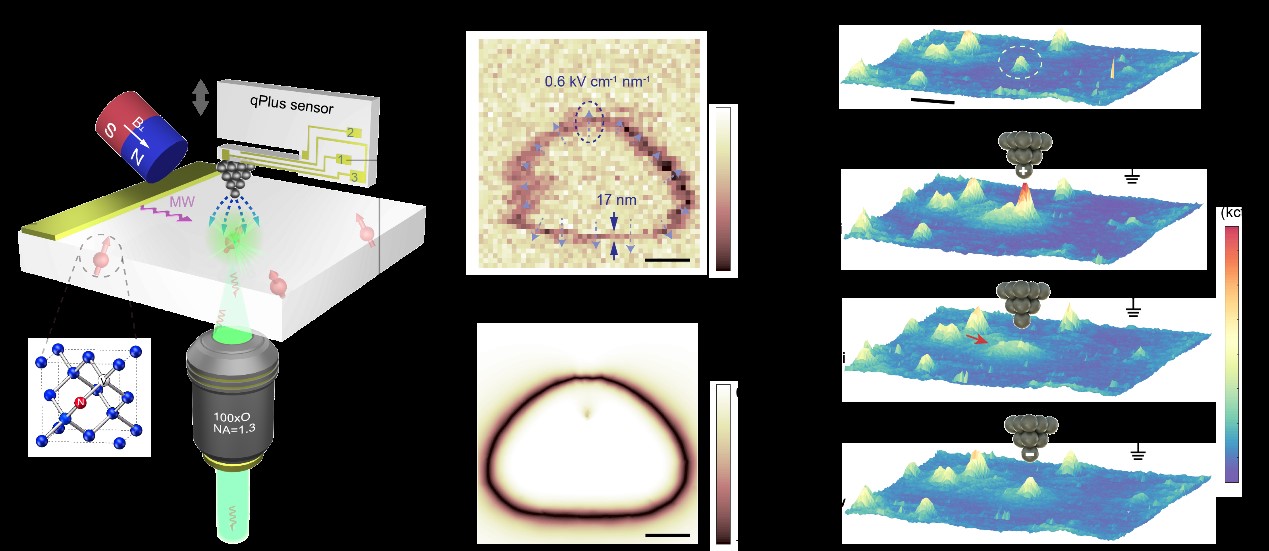
Figure: a) Schematic graph showing the NV-based scanning electrometry. b) and c): The experimental and simulating electric-field mapping of a sharp metal tip through the single shallow NV. d) Charge-state control of single NV by the local electric field of tip.
Using this new system, the team also realized the reversible control of single NV’s charge states (NVˉ, NV+ and NV0), where NVˉ is used as the quantum sensor, while NV+ and NV0 are basic building blocks of quantum storage for improving the signal-to-noise ratio of quantum sensing. The researchers found that, with the assistance of the photon ionization by the excitation laser, the local electric field of a sharp biased tip can be applied to achieve the local polarization/depolarization of the diamond surface and induce the charge-state switch of NV with nanoscale accuracy (down to 4.6 nm). This finding will help to purify NV’s immediate electrostatic environment, enhance the NV coherence and build up NV-based quantum networks.
Read the original article on Peking University.

