Carbon nanotubes are a promising type of materials with potential uses in applications such as light-emitting diodes, single-electron transistors, or as single photon sources. They are essentially tubes made up of graphene twisted in specific ways, and the way they are twisted is critical for allowing the desired properties to emerge. Creating devices with desired properties requires precise manipulation of the position and orientation of the nanotubes, along with a property known as “chirality,” which essentially describes how much it is twisted. It is difficult to manipulate the molecules precisely, however, as using solvents or high-temperature treatment inevitably leaves the nanotubes dirty, hampering their optical characteristics.
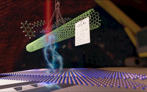
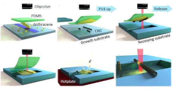
To solve this issue, the researchers looked for a way to engineer the nanotubes without using solvents. They experimented with using anthracene, a chemical derived from oil, as a sacrificial material. Essentially, they picked up the nanotube on a scaffolding of anthracene to carry it wherever they wanted, and then used heat to sublimate the anthracene, leaving the nanotube in an optically pristine condition. They also developed a method for monitoring the photoluminescence of the nanotubes during the transfer, ensuring that a nanotube with the desired optical properties would be placed at a right location.

Taking a single carbon nanotube and positioning it precisely.
The group confirmed that following the dry transfer, the remaining nanotubes has bright photoluminescence, up to 5,000 times as bright as the original molecule, a quality that makes them ideal for optical devices. In addition, the group was able to precisely position the nanotube on top of a nanosized optical resonator, enhancing the light emission properties.
According to Keigo Otsuka from the RIKEN Cluster for Pioneering Research, the first author of the paper, “We believe that this technology could contribute not only to the creation of nanodevices from carbon nanotubes with desired properties, but also to the construction of higher-order systems that are based on the free combination of atomic layer materials and other nanostructures.”

Schematic showing how the carbon nanotube is constructed and positioned.
“Beyond that,” says Yuichiro Kato, the leader of the group, “this technology has the potential to contribute to the development of atomically defined technologies that go beyond nanotechnology, in which materials with precise structures at the atomic level are used as building blocks to design and build functions that are different from those of existing materials.”
Read the original article on Riken.


