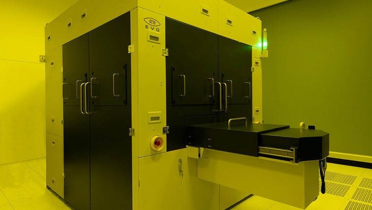
EV Group (EVG), a leading supplier of wafer bonding and lithography equipment for the MEMS, nanotechnology and semiconductor markets, today announced the EVG®770 NT—its next-generation step-and-repeat nanoimprint lithography (NIL) system. The EVG770 NT enables precise replication of micro- and nano-patterns for large-area master stamp fabrication used in high-volume manufacturing of augmented reality (AR) waveguides, wafer-level optics (WLO) and advanced lab-on-a-chip devices.
Until now, further developments and production scaling requirements for step-and-repeat NIL have often been limited by the availability of precise masters on larger areas. Leveraging EVG’s decades of experience in NIL and step-and-repeat mastering, the EVG770 NT has been designed as a fully production-oriented system to maximize performance, productivity and process controllability. It provides industry-leading overlay accuracy and resolution with scalability up to 300-mm-wafer and Gen-2-panel sizes. As a result, customers can now realize the promise of high-volume, cost-efficient and high-fidelity NIL patterning.
Benefits of Step-and-Repeat NIL
WLO, one of the main markets driving NIL adoption, has enabled completely new applications for mobile consumer electronic products—from improved autofocus for smartphone digital cameras and facial recognition for added smartphone security to 3D modeling and imaging enhancements for AR and virtual reality (VR) headsets. Step-and-repeat NIL enables cost-effective production of WLO as well as small structures used in microfluidic devices by taking a master mold of a single die that has been written with an electron beam or other technologies and replicating it multiple times across a substrate to create full-area master templates and stamps. The resulting step-and-repeat master can then be used to produce working stamps for subsequent wafer-level and panel-level manufacturing.
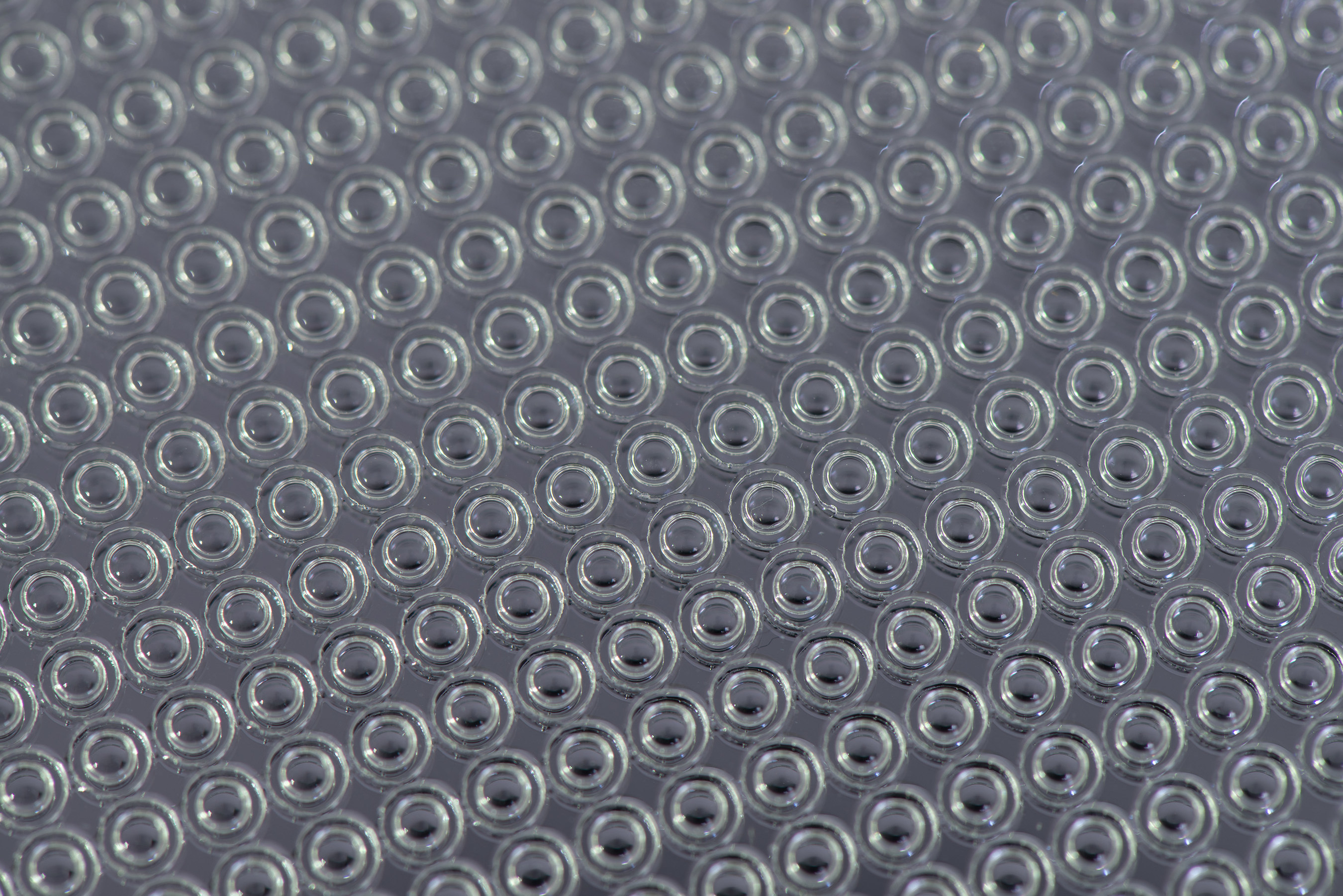
Closeup of 300-mm step-and-repeat master for wafer-level optics.
The ability to replicate larger master molds over ever-larger substrates allows more devices to be produced simultaneously as well as allows for the production scaling of larger individual devices without stitching. This approach offers significant yield and cost advantages compared to conventional mastering processes, such as diamond drilling, laser direct writing and electron-beam writing, which are difficult to scale up to larger substrates due to their low throughput and high cost of implementation. Incorporating the step-and-repeat process enables the use of best-performing dies and the ability to efficiently bring these high-quality patterns into production lines.
"EV Group has invested more than a decade in developing and refining our step-and-repeat mastering technology to bring the manufacturing benefits of NIL to a wider range of markets and applications," stated Dr. Thomas Glinsner, corporate technology director at EV Group. "The result of that effort has led to the EVG770 NT, which provides the missing link bridging free-form micro-optics or high-fidelity nanopatterning with cost-efficient large-scale production requirements. With this breakthrough step-and-repeat solution, our customers now have the ability to create their own master templates and bring the entire NIL process flow in-house, providing them with greater flexibility and faster turn-around on their production runs. For customers wishing to explore the use of NIL for new products or that have small production needs, EVG offers step-and-repeat mastering services within our NILPhotonics® Competence Center—our open access innovation incubator for customers and partners that shortens the time to market for innovative photonic devices and applications."
Breakthrough in Performance and Scalability
The EVG770 NT includes several features that aid in both process development as well as production:
- Stitchless replication of single lens/die templates up to 80mm x 80mm onto substrates up to 300-mm wafers and Gen-2 (370mm x 470mm) panels
- Sub-250-nm alignment accuracy and sub-50-nm resolution
- Enables a working-stamp high-volume-production process that avoids wear-out of the expensive original templates
- A new exposure source design with higher dose that significantly reduces exposure times
- Inspection microscopes and live process camera feeds to verify and monitor process results on the go
- Non-contact air bearings to minimize particle contamination
- Automated substrate loading and stamp changing unit with storage buffer for five stamps
- In-situ control and characterization of imprinting and detachment forces
- Software upgrade to EVG's latest Computer Integrated Manufacturing (CIM) Framework platform used across EVG's high-volume-manufacturing process equipment
Product Availability
The EVG770 NT has already been shipped to select customers and EVG is now accepting orders for the new system. EVG is also offering tool demonstrations and step-and-repeat mastering services on the new system at its NILPhotonics Competence Center at EVG's headquarters. For more information on the EVG770 NT step-and-repeat NIL system, visit here.
EVG at SPIE Digital Optical Technologies
EVG will present an invited paper on the benefits of NIL in manufacturing high refractive index waveguides at the SPIE Digital Optical Technologies Conference being held online on June 21-25.
Read the original article on EV Group (EVG).

