The material, known as biphenylene network, is highly conductive and may prove able to store more electrical energy than even graphene, the astonishing atomic-thickness carbon honeycomb material identified nearly 20 years ago.
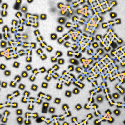
In May, scientists announced that they have been able to tailor the arrangement of carbon atoms into a mesh that, for the first time, includes hexagons, squares and octagons, while ensuring the material is still only one atom thick.
The new geometric arrangement in two dimensions adds to the list of different carbon structures – or allotropes – such as graphite, diamond and graphene. But scientists have found it has very different electronic properties.
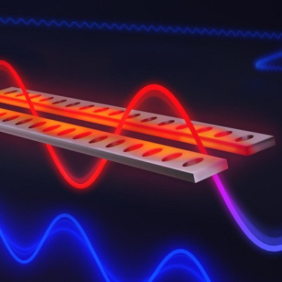
It makes sense to compare the new material with graphene, where carbon atoms bond in a single layer of hexagons to form a mesh with astonishing electrical and thermal characteristics, as well as outstanding mechanical strength, and yet is highly transparent.
Laboratory research on the new material at University of Marburg in Germany and Aalto University in Finland has found that biphenylene network ribbons a few atoms wide behave electrically like a metal. That gives a hint that the material may be developed to make conducting wires in carbon-based electronic circuits.
‘If you take similar-width graphene nanoribbons, then they are typically semiconductors and this biphenylene is more readily a metal,’ said Peter Liljeroth, professor in the department of applied physics at Aalto University. That could make the material useful as a nanoscale conductor in future electronic devices, he added.
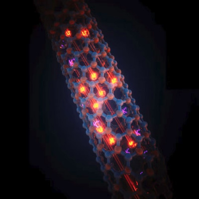
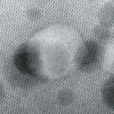
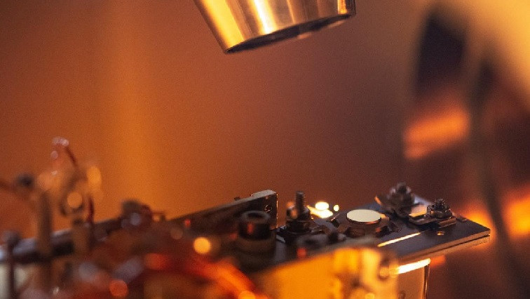
He and his team made their findings using an imaging technique called scanning tunnelling spectroscopy to scrutinise strips of biphenylene network up to 21 atoms wide. Those ribbons were made by Prof. Michael Gottfried’s group in the physical chemistry department at Philipps-Universität Marburg, in Germany.
The Marburg team developed the synthesis route for this material. They made molecular chains containing carbon in specific arrangements that gather on an ultra-smooth, non-reactive gold surface. And then another step – dubbed ‘HF-zipping’ – meshes the chains together to form the biphenylene network strips.
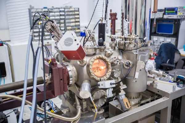
Peter Liljeroth and his team made their findings using an imaging technique called scanning tunnelling spectroscopy to scrutinise strips of biphenylene network up to 21 atoms wide.
Electrical potential
Analysing larger-scale samples could help to show if a biphenylene anode could increase the efficiency of lithium-ion batteries, commonly used in mobile phones and electric vehicles.
‘If you have bulk or multilayer biphenylene… then there are theoretical predictions that the lithium storage capacity should be higher, much higher, than for graphene,’ Dr Liljeroth said.
If confirmed, that would make the material hugely attractive in rechargeables. But Prof. Liljeroth emphasises there is a very long way to go before such properties may be potentially harnessed in industrial or consumer applications.
A challenge in making bulk biphenylene is to increase the accuracy of the synthesis process of zipping together strips or ribbons of biphenylene of sufficient quality to form larger sheets, without parts of the material defaulting to graphene as the carbon atoms aggregate and bond.
While the Aalto researchers could identify the electrical properties of the material from Marburg, other characteristics of biphenylene network remain unexplored. Research is still needed to nail down its mechanical, thermal and optical qualities. To do that, it would help to have bigger samples.
Carbon wires
The confirmed metallic conducting properties already point to the possibility of conducting wires for electronics at the smallest scale.
Wires made of metals such as copper typically degrade at atomic thicknesses through a process of electromigration – where moving electrons can displace atoms and damage the wires, which become unstable and eventually break.
A material such as biphenylene network could help to avoid these difficulties in electronic circuits, working like a metal in conducting electrons, but without the drawbacks. That would make for more stable conductors, allowing smaller wires to be used in nanoscale electronics.
‘This is one of the problems that has to be overcome or solved, and carbon-based materials are quite good in this respect,’ Prof. Liljeroth said.
But he added a clear note of caution: ‘There are many, many steps in between now and actually using this in a microprocessor.’
These properties, and others yet to be identified, could provide rich fields for exploration and development, as could the novel way of producing the biphenylene network itself.
Prof. Liljeroth emphasised the potential for the HF-zipping approach used by Prof. Gottfried’s team to make any number of other carbon structures.
Zipping ribbons
The Marburg team used carbon-based precursor chemicals containing hydrogen and fluorine to “zip” together different atomic carbon chains. Rather than defaulting to graphene – the most basic form on the surface – the extra step involved chemically tailoring the edges of the ribbons that zip together to form the biphenylene network.
‘What I hope comes out of this work is that people start to think about this kind of HF- zipping process to make new materials, (so) you can start with the same concept, tweak the precursors and end up with another 2-D carbon network,’ Prof. Liljeroth added.
Since the material has so far been produced on a gold surface, another challenge is to perfect the transfer of the biphenylene network off the metal. That is a task where the researchers may draw lessons from work done on graphene – a material where ongoing work also offers some other pointers for developing biphenylene network.
‘I would say there's a lot of potential … now that they have shown that these structures are feasible, they are stable, at least under these conditions,' said Professor Roman Fasel, who heads the nanotech@surfaces Laboratory at the Swiss Federal Laboratories for Materials Science and Technology (EMPA) and was not involved in the research.
‘This is going to be really challenging to scale up,’ he said, but added that work on graphene had shown it was possible to progress from the tiniest specks of material to workable scales.
‘One direction is to optimise the synthesis to achieve a large area 2-D network, let's say for electrodes and things like that, but the other would be to find a way to make well-defined nanoribbons – so just the 1-D variant of the material,’ he said.
One of the main challenges facing biphenylene is identifying properties that make it an obvious choice for future applications – known in computing terms as a ‘killer app’ – where it is vastly better than rivals, as well as easier and cheaper to make.
After all, people have been working on graphene for nearly two decades and though it exhibits many outstanding properties and has found uses in paints and coatings, microelectronics and transparent conductors – as well as being used in tennis rackets and ink – it has not completely revolutionised any particular field.
‘In some cases, a new material opens up something that was simply not possible to do with the existing technology, and then it can break through faster,’ said Prof. Liljeroth. ‘But I don't know about biphenylene -- we'll have to see about that.’
Read the original article on European Commission.