These days, however, silicon transistors are so atomically small that soon it may not be possible to shrink them. That’s why researchers are investigating new, more efficient materials with the potential to replace silicon.
One leading candidate is carbon nanotubes, which are tiny, rolled-up pieces of the practically 2-dimensional wonder material graphene. When used as transistors, the nanotubes could be five times as energy efficient and five times faster than silicon. The problem is that working with the tiny tubes — just nanometers in diameter — is difficult. To be useful as transistors, they need to exhibit uniform electrical characteristics, be aligned in the same direction, and be closely, but not too closely, packed together.
UW–Madison engineers have worked out a method to make orderly sheets of 2-dimensional carbon nanotubes by aligning them between layers of water and a solvent “ink.”
Researchers have struggled to find techniques to precisely deposit the tubes, but engineers at the University of Wisconsin–Madison have discovered a new method of aligning the nanotubes by turning them into 2D liquid crystals. They described their research in the journal Science Advances.
“In this new technique we are able to align carbon nanotubes across industry scales,” says Katherine Jinkins, first author on the paper.
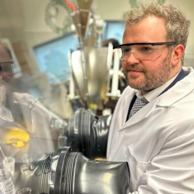
Jinkins, advised by Michael Arnold, a UW–Madison professor of materials science and engineering at UW–Madison, graduated with her doctorate in July 2020.
“In as little as 40 seconds, we can coat an entire 4-inch wafer with a uniform array of highly aligned carbon nanotubes,” she says. “That fills a void that has existed in the carbon nanotube community for almost 30 years.”
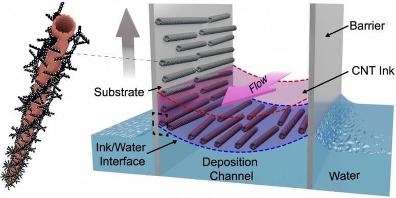
The technique was a serendipitous discovery. While trying to understand some previous research, the team deposited nanotubes suspended in a solvent over a layer of water. But the researchers noticed that the nanotubes began to self-organize and align at the interface between the liquids.
“We didn’t understand why, so this became the focus of four years of research by Katy to get to the bottom of it,” says Arnold. “Once we understood what was going on, then it could be engineered into a process that might be useful to industry.”
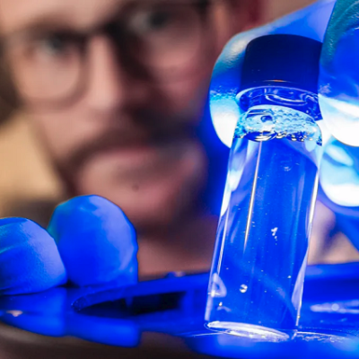
In the fabrication technique, the team sorts and purifies commercially produced nanotubes using techniques previously utilized by the Arnold group. This purification process produces nanotubes in solvents, or nanotube inks, which they then flow at a constant velocity and thickness over a layer of water. At the interface between the ink and water, the nanotubes begin to concentrate and self-organize, forming a liquid crystal. That liquid crystal is then transferred on a substrate moved through the ink and water interface. The result is a wafer covered in trillions of highly aligned carbon nanotubes.
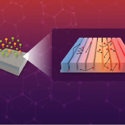
Using Raman spectroscopy, the team was able to confirm the nanotube density is near that needed for electronics, and using scanning electron microscopy they also determined the alignment of the tubes to be within 6° locally. This almost ideal nanotube ordering led to excellent electrical properties that were confirmed consistent across the entire wafer.
The process is a big advance for carbon nanotube research. However, it does need some tweaks before nanotube computer processors end up in smartphones and laptops. The industry standard is 12-inch wafers, so the process, patented through the Wisconsin Alumni Research Foundation, needs to be scaled up while maintaining the uniformity of the nanotube alignment. The team hopes to improve the alignment even more, and also aims to increase the density of the nanotubes while making sure they don’t cross one another, which is another challenge.
The result, however, will be worth it.
“If we can solve all these challenges, then we’ll be able to make computer chips from nanotubes that are better than silicon by a significant margin,” says Arnold. “The other cool thing about nanotubes is if you suspend them in a solution, like we’re doing, then you can deposit them in multiple layers, like 3D integrated circuits. That would allow us to increase the number of transistors significantly. The payoff could be enormous—if we can figure this all out.”
Read the original article on University of Wisconsin–Madison.