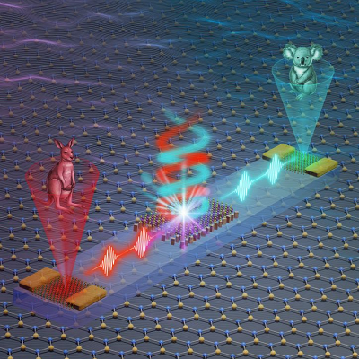
What is Nanofabrication
Nanofabrication is a cutting-edge technology that is used to manufacture high-tech microchips, microcontrollers, and other silicon devices. Nanofabrication is also attracting the attention of scientists in the military, aerospace, and medical fields. When compared to large devices, nanofabrication is concerned with the properties of atoms in a material and finding solutions to save space, time, and money.
Integrated circuits (ICs), which have been a fundamental aspect of electronic devices for decades, have evolved as a result of the advancement of nanofabrication. Circuits are being manufactured atom by atom, analogous to how a house is produced brick by brick, using programmable nanomachines.
But According to FourCreeds, There is no universally acknowledged definition of nanofabrication, nor is there a clear distinction between nanofabrication and microfabrication. New tools and techniques are constantly being developed to tackle the ongoing challenge of lowering component size in microelectronics. Component sizes dropped from tens of micrometres to single-digit micrometres, hundreds of nanometers, and finally a few tens of nanometers, where they are now. As a result, what was formerly known as microfabrication has been renamed nanofabrication, despite the fact that the underlying concepts have remained mostly the same. The fabrication of integrated circuits has been the primary driver of this technology, although there have been significant spillover effects in other sectors, including photonics.
Classification
Thin films, lithography, and etching are three important aspects of nanofabrication that can be loosely classified. Each of these topics is huge in and of itself, but in this chapter, we strive to convey the fundamental concepts in a simple manner for someone who is unfamiliar with them.
The purpose is to provide a general grasp of what these areas are as well as the benefits and drawbacks of the most often utilised procedures, rather than to provide a practical experience that allows one to walk into a laboratory and accomplish these activities. It is hoped that it would serve as a foundation for additional particular instruction for anyone interested in delving deeper into these topics.
1) Thin Film Nanotechnology
A thin film is a material layer that ranges in thickness from fractions of a nanometer (monolayer) to several micrometres. The method of “deposition” is used to make thin films. The Deposition is a thin-film coating process that involves changing the states of matter from solid to liquid to vapour to plasma.
A multitude of vacuum procedures can be used to achieve this. Chemical vapour deposition (CVD), physical vapour deposition (PVD), evaporation through vacuum sublimation, and occasionally a mixture of these technologies are used in vacuum deposition processes. These are just a few examples of how a thin film can be created.
Thin films are everywhere. Electronic semiconductor devices are one application that benefits from thin-film technology. Integrated circuit chips, micro-fabricated mechanisms, micro-electromechanical systems (MEMS), micro-electronic optical systems, and light-emitting diodes are all examples of this (LEDs). Optical coatings, photovoltaic solar cells, and thin-film batteries are some of the more common applications.
When thin film optical coatings (e.g. anti-reflective, or AR, coatings) are made up of many layers with different thicknesses and refractive indices, their performance is often improved. A superlattice, which leverages the phenomenon of quantum confinement by constraining electronic events to two dimensions, can be formed by a periodic structure of alternating thin films of different materials.
Computer memory is made out of ferromagnetic and ferroelectric thin sheets.
Thin film technology is being investigated as a way to significantly lower the cost of photovoltaic systems, which capture solar energy.
Thin-film batteries can be deposited on any shape or size chip or printed on plastic, thin metal, or paper using thin-film printing technology. The production of reflective, anti-reflective, or self-cleaning glass is a frequent application of thin-film technology.
2) Lithography
Lithography is the primary method for fabricating nano-components with extremely small feature sizes. Optical lithography is the most widely used technology today, and with the usage of 157-nm and 193-nm wavelength tools, it is predicted to be important beyond 70 and 100 nm.
More advanced lithography methods will be required to reduce feature sizes to 50 nm and below. The candidate for the future of microelectronics is extreme ultraviolet (EUV) lithography, which is currently widely accepted. EUV lithography will achieve feature sizes of 45 nm and below at a wavelength of 13 nm. Photolithography, scanning lithography, soft lithography, and other miscellaneous techniques are the four groups of NL technologies.
2-1) Applications and Properties of Photolithography
Photolithography is a selective procedure for patterning a needed design onto the material that will be utilised to build using (the wafer in the semiconductor sector). A photoresist is used as the first stage, followed by the application of a pattern in an even film. The mask is a metal sheet that holds the actual pattern that will be etched into the photoresist later on.
After illuminating the photoresist with UV light from behind, this mask is sliced so that the exposed sections of the photoresist become the true pattern. The exposed pieces will either stay on the produced device (negative resist) or can be wiped away later (positive resist).
With photolithography being the most important constraint on wafer size, this is the area where the majority of research has been focused. Contact printing is the earliest form of photolithography. The mask was directly positioned on top of the photoresist during the exposure process in this configuration. While this method gave outstanding resolution, it did occasionally result in minor damage to the mask and wafer.
Projection printing, the next innovation, was able to detach the mask from the photoresist and solve the difficulties.
2-2) Lithography using an electron beam (e-beam)
Currently, electron-beam lithography, or EBL, is the most successful technology for creating patterns on substrates, such as X-ray masks and photomasks, and is utilised to make the tiniest parts on silicon substrates. Electrons are used to etch the photoresist directly. A computer directs the electrons’ route through a series of lenses and coils to expose the correct parts of the photoresist.
Elaborating a matrix of a micro-fabricated e-gun for an e-beam masker is the focus of efforts for next-generation e-beam lithography. The major goal is to make electron beam lithography more parallel.
2-3) X-Ray Lithography
X-ray lithography uses the same process as UV lithography, but instead of UV, an X-ray source is used.
3) Nanofabrication Etching
To develop the necessary three-dimensional nanostructures, surfaces can be subjected to an etching agent after photolithography. The etching agent will wear away the uncovered portions while the areas covered by the resist will be protected; this process is known as etching in the field of nanofabrication.
Etching is a nanofabrication technique that involves chemically removing layers from a wafer’s surface during the production process. Etching is a vital process module, and each wafer goes through a number of etching steps before being finished.
A “masking” substance that resists etching is used to protect part of the wafer from the etchant during multiple etch stages. In some circumstances, the masking material is a photoresist that has been photolithographically patterned. In other cases, a more robust mask, such as silicon nitride, is required.
Etching is a critical step in nanofabrication that removes the substrate or extra material that has been placed down on the surface before. The word comes from the Dutch “etsen,” which means “to etch with acids on material surfaces,” and the German “ätzen,” which means “to eat away.” Although it is difficult to say who was the first to utilise etching as a technique, etching was used to adorn jewellery during the reign of Egypt’s Queen Cleopatra (69-30 BC). After printing from iron plates in 1513, Swiss artist Urs Graf became renowned as an early pioneer of etching. Today, scientists and engineers use the process to generate nano-scale designs that are used in a variety of technologies that help us live better lives.
Wet and dry etching are the two basic forms of etching used in nanofabrication. While the main difference between the two procedures is the etching agent utilised, which is either “liquid-phase” in wet etching or “plasma-phase” in dry etching, both entail the removal of layers from a masked surface to achieve three-dimensional nanostructure transfer.
Read the original article on FourCreeds.