Everything in our modern world relies on computers, be it for your personal entertainment or the stock exchange, from simple accounting to the regulation of national power grids. You yourself are probably carrying a computer with you right now in form of your smartphone, which is, simply put, nothing more than a sophisticated calculator. The increasing computerization and its benefits are the results of over half a century of intense research and improvements in the fields of semiconductor physics and computer sciences.
Unlike modern computers, the first ‘automatic calculators’ were huge unwieldy machines based on vacuum tubes, using punching cards for the execution of commands. Nowadays, the same calculational power these old computers possessed fits right into one of your hands.
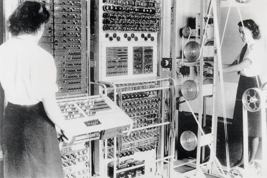
A Colossus Mark 2 computer, 1943. It operated via vacuum tubes and was used to decipher german communications during World War II.
The transistor
As with all revolutionary technologies, computer technology started with a rather plain invention. The most basic building block of a computer is called a transistor. The first functioning transistor was developed in 1947 by Shockley, Bardeen and Brattain at Bell Laboratories in the US. It was a rather crude looking, point-contact transistor prototype consisting of a germanium crystall and a few gold contacts. And, as shown in the image below, it was quite large, given that microchips weren’t a thing back then.
But soon, scientists and engineers from all over the world tried to improve and invent new types of transistors, making them faster, smaller and less energy consuming. The integration of these transistors into regular arrays gave birth to integrated circuits, modules that could perform a plethora of logic operations and calculations. You know them as ‘microchips’.
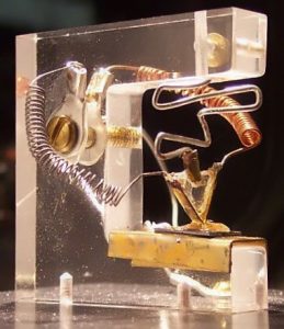
Replica of the first transistor made by Schockley, Bardeen and Brattain in 1947.
Now the improvement of integrated circuits over the timespan of the last century is a natural thing, driven by economic and scientific factors. For example, the introduction of new key fabrication technologies, allowing for higher transistor densities, or the decrease in production cost, resulting in an increased integration of microchips in, well… everything that was mentioned in the beginning of this blog post plus more.
Moore’s law
Rather than a scientific law, Moore’s law describes the development of transistor densities on integrated circuits as an empirical projection. It predicts that the number of transistors in a dense integrated circuit doubles about every two years. Over time, Moore’s Law has become somewhat of a self-fulfilling prophecy, a commitment the semiconductor industry has imposed upon themselves when it comes to increasing the transistor density on integrated circuits.
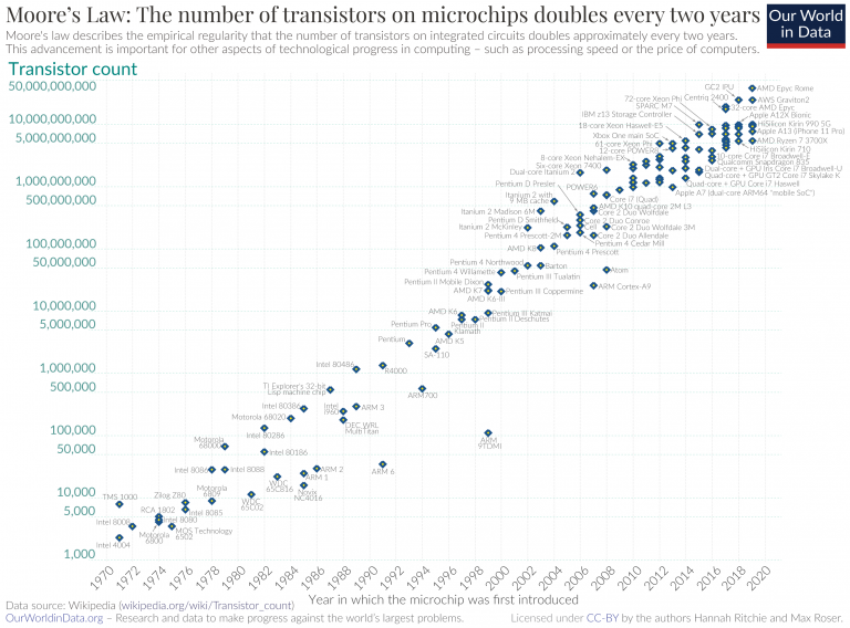
A semi-log plot of transistor counts for microprocessors against dates of introduction, nearly doubling every two years.
In order to understand how smaller transistors lead to more powerful computers, I’d like for you to imagine a three-dimensional square block. This block is our transistor and can perform a certain number of ‘operations’ or switching between ‘on’ and ‘off’ state at a certain speed. Now assuming we can somehow manage to decrease the size of the block to half of its original size in all dimensions, you can now fit eight of these smaller blocks into the space the original block needed. With this, we have effectively increased the number of operations we can fit into a predefined volume by a factor of eight. Additionally, there are a few beneficial side effects of the downscaling of our transistor: The device needs less energy and has a faster response time, since it is smaller. Of course, this is a very simplified picture, but the general notion is exactly that.
However, after this thought experiment we need to ask ourselves a very fundamental question: How small can we make our transistor? And is there a limit? Certainly the theoretical limit would be the atom, realistically speaking a few hundred atoms, as famous physicist Richard Feynman pointed out in one of his lectures. At the same time, Feynman said that there’s still ‘plenty of room at the bottom’, referring to the possible advancements seminconductor fabrication could hold in the future.
Today, the smallest feature in a transistor, the gate oxide layer, steadily approaches the 3 nm mark. This corresponds to not even a dozen atoms in thickness! The reality the semiconductor industry faces nowadays is that it becomes increasingly more difficult and expensive to scale down transistor technology any further. The current instrumentation is approaching a limit as in what is feasible and so is the transistor. Of course, one will have to consider completely alternative technologies for single-atom computation if you wish to explore the quantum realm. What stands beyond classical silicon technology based computation however will not be covered in this blog post. Instead, let us return to a more fundamental economic problem the industry faces: fabrication cost. The fabrication cost and the related development of production lines capable of producing features small enough has become increasingly expensive, to a point where only the largest semiconductor companys can afford such a venture.
Introducing block copolymers
There exist several concepts based on so called ‘bottom-up’ manufacturing as opposed to the currently used ‘top-down’ approach in nanofabrication. ‘Top-down’ describes the successive removal of material from a large sample in order to achieve small structures, while ‘bottom-up’ techniques utilize inherent properties of particles and molecules to self-assemble to build up defined nanostructures. Self-assembled nanostructures thus offer an inexpensive, facile route for nanofabrication of transistors.
One of those (macro-)molecules that can be used for self-assembly are so called block copolymers (BCP). Block copolymers consist of two different long molecular chains which are connected with each other by a covalent bond. If these polymer chains have a negative affinity towards each other, the BCP will attempt to demix. Since the chains are connected with each other however, microphase separation will instead occur, a process which results in a defined microstructure with domains consisting of single blocks. The idea is to use this property of BCPs to fabricate defined masks and structures in an inexpensive way that can be used in photolithography for semiconductor fabrication.
The process of producing a BCP film with defined microstructure can be divided into several steps. First, a thin unordered film of BCP is produced, usually by spin-coating a solution containing the BCP onto a substrate and letting the solvent evaporate. Then, the BCP film is annealed, for example at elevated temperatures. The annealing step is necessary, since it allows for the chains of the BCP to disentangle and separate into microphases. By selecting the blocks and block lengths of the BCP, as well as annealing conditions and film thickness, one can influence the resulting microstructure.
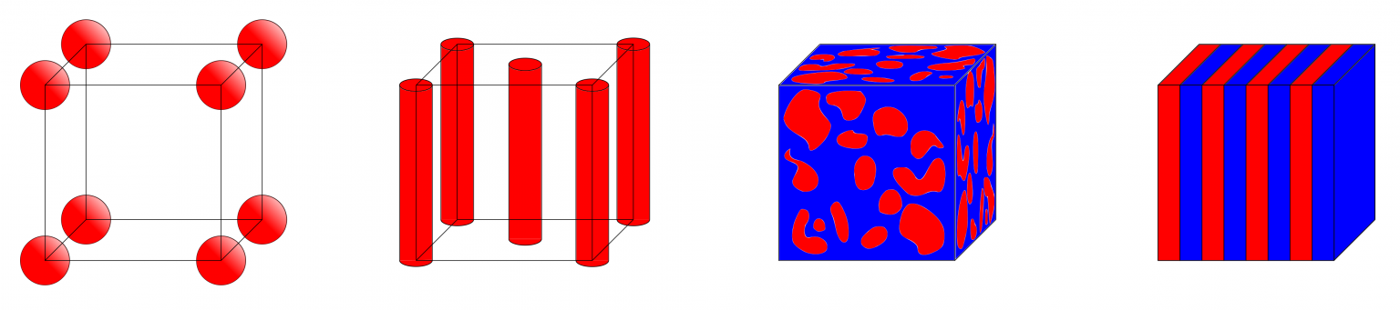
Different microphases that may form during microphase separation of BCPs, depending on the individual block lengths of the copolymers, as well as their interactions and the temperature. From left to right: cubic, cylinders, gyroid, and lamellar phases.
Directed self-assembly
However, the resulting microstructures have no preferred orientation. Not simply annealing, but directional annealing is necessary for achieving defined and oriented microphase separated nanostructures. Directed self-assembly utilizes the substrate affinity the BCP has by tweaking the interaction parameter between substrate and BCP. This can be done using chemical methods (chemoepitaxy) or pysical methods (graphoepitaxy).
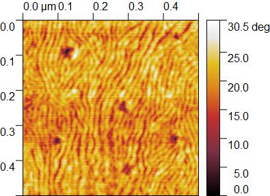
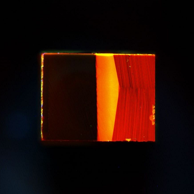
AFM phase image of aPolyethylene-block-polyethylene oxide film after thermal annealing showing a lamellar structure.
Chemoepitaxy describes altering the surface interactions between BCP and substrate by functionalization or coating of the substrate surface. The functionalized surface may have a selective affinity towards only one block of the BCP, leading to preferred wetting of the particluar block on the substrate, and thus inducing an orientation of the polymer chains.
This method can be combined with graphoepitaxy, which uses physical guiding patterns (e.g. trenches) to induce a macroscopic orientation over large areas. The patterns themselves are relatively large (hundreds of nanometers), and easy to fabricate. However, within these guiding patterns, the BCP experiences a confinement, which induces well-ordered microseparated structures over large areas. By further processing of annealed BCP films via lithographic or etching techniques, defined nanostructures can be produced.
The future of BCPs
Despite the large amount of research covering BCP directed self-assembly, this technique is unlikely to be adapted in high-volume semiconductur manufacturing in the near future. There remain many open questions and challenges concerning the reproducability of directed self-assembly, as well as the stability and processability of assembled BCP microstructures. The mechanism of defect formation, including interfacial effects caused by substrate-BCP interactions, is not yet fully understood. The complicated kinetics of soft matter often leads to high defect densities. Especially below the 10 nm regime, lacking elaborate characterization procedures for high-volume, on-the-fly analysis makes current application unlikely. Precise control over annealing conditions is therefore necessary and could open a path for large scale application of BCPs in seminconductor fabrication.
Read the original article on Helios Blogs.