From the discovery of microorganisms in the field of biology to imaging atoms in the field of physics, microscopic imaging has improved our understanding of the world and has been responsible for many scientific advances. Now, with the advent of spintronics and miniature magnetic devices, there is a growing need for imaging at nanometer scales to detect quantum properties of matter, such as electron spins, magnetic domain structure in ferromagnets, and magnetic vortices in superconductors.
Typically, this is done by complementing standard microscopy techniques, such as scanning tunneling microscopy and atomic force microscopy (AFM), with magnetic sensors to create “scanning magnetometry probes” that can achieve nanoscale imaging and sensing. However, these probes often require ultrahigh vacuum conditions, extremely low temperatures, and are limited in spatial resolution by the probe size.
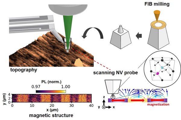
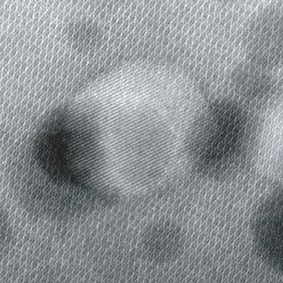
Scanning diamond NV center probe fabricated by FIB milling demonstrates imaging of magnetic domain structure of magnetic tape.
In this regard, nitrogen-vacancy (NV) centers in diamond (defects in diamond structure formed by nitrogen atoms adjacent to “vacancies” created by missing atoms) have gained significant interest. The NV pair, it turns out, can be combined with AFM to accomplish local magnetic imaging and can operate at room temperature and pressures. However, fabricating these probes involve complex techniques that do not allow for much control over the probe shape and size.
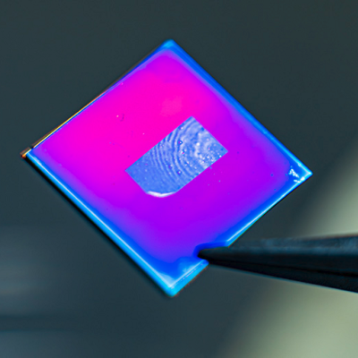
In a new study led by Associate Professor Toshu An from Japan Advanced Institute of Science and Technology (JAIST), and Yuta Kainuma, a Ph.D. student at JAIST, in collaboration with researchers from Kyoto University, Japan, and the National Institute of Advanced Industrial Science and Technology, Japan addressed this issue, fabricating NV-hosting diamond probes using a novel technique combining laser cutting and focused ion beam (FIB) processing that enabled both a high degree of processing freedom and control over probe shape. This paper was made available online on 28 December 2021 and was published in Volume 130 Issue 24 of the Journal of Applied Physics.
To begin with, the team created N-V centers in bulk diamond by implanting nitrogen ions into it. Next, they polished the opposite surface and produced multiple rod-shaped pieces with laser cutting. They attached one of the diamond rods to the tip of an AFM probe and used FIB processing to turn the front surface of the diamond rod into the final probe shape. “FIB uses gallium ions to shape the probe. However, these ions can create vacancies in the diamond structure altering the charge state of the NV defect. To avoid this, we used a donut-shaped milling pattern around the center of the probe to prevent any damage to the NV center,” elaborates Dr. An. The final probe was a micropillar consisting of 103 NV centers with a diameter of 1.3 µm and a length of 6 µm.
Using the probe, the team imaged the periodic magnetic domain structure in a magnetic tape. “We imaged the stray magnetic fields from the magnetic domain structure by mapping the photoluminescence intensity at a fixed microwave frequency and the resonance frequencies in the optically detected magnetic resonance spectra,” explains Dr. An.
The team is optimistic that the new fabrication method will broaden the applicability of quantum imaging probes. “In recent years, the development of new devices have been sought to solve environmental and energy problems and realize a sustainable prosperity of human society. Quantum measurement and sensing technology is expected to completely reform the system that supports the social infrastructure in the future. In this regard, our fabrication technique could help boost efforts in realizing nano-scale quantum imaging,” speculates Dr. An
Who knows, the future might indeed be quantum!
Read the original article on EurekAlert.