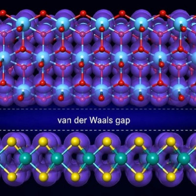
The most widespread method for the synthesis of 2D-2D heterostructures is the direct growth of materials on top of each other. 2D structures are atomically thin layered materials that can be stacked to build functional heterostructures. In such structures built by atomic deposition, 2D layers are weakly bonded by van der Waals interactions and can be taken apart in some solvents or thermal processes. The lack of control over the interface of the two materials in terms of electronic communication, chemical nature or interlayer distance thus impedes the construction of robust multi-purpose devices.
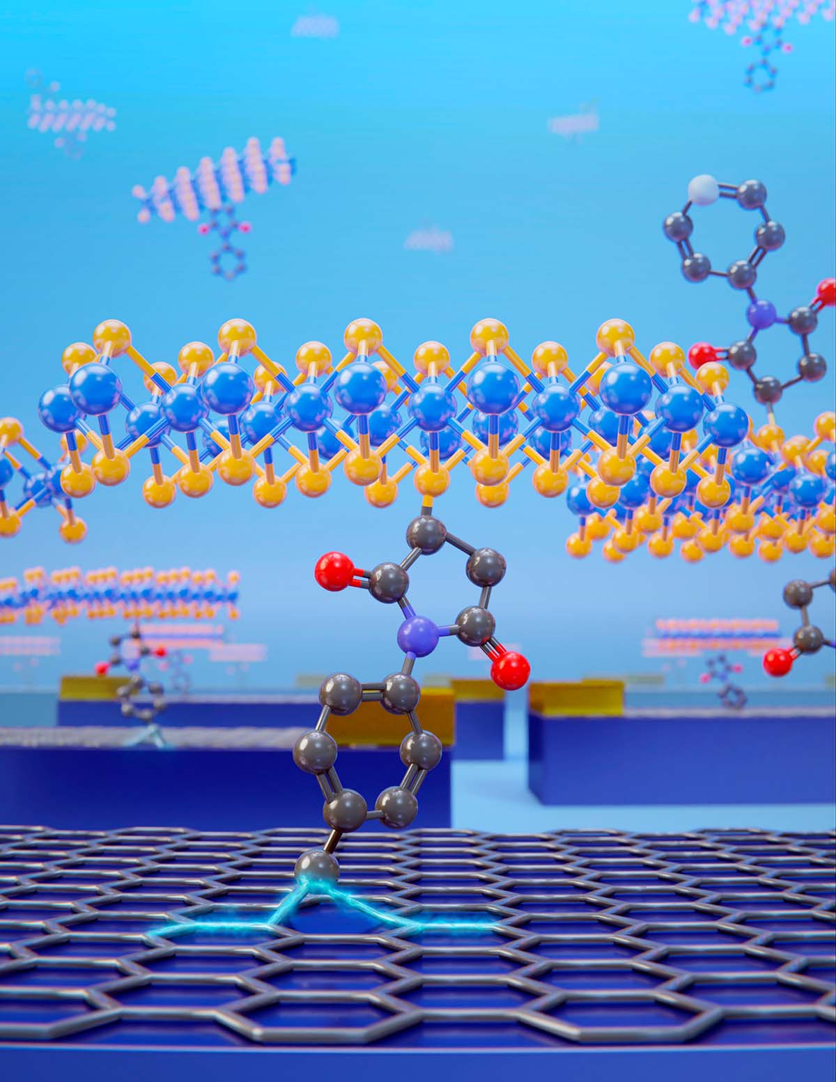
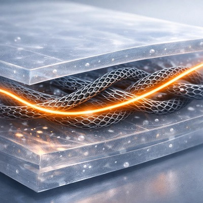
2D structures of MoS2 are connected to graphene using a covalent bond.
A team of researchers led by Enrique Burzurí and Emilio M. Pérez at IMDEA Nanociencia (Madrid, Spain) have connected covalently for the first time layers of 2D materials: MoS2 and graphene. The team has used the tools of synthetic chemistry to sew several flakes of MoS2 to single-layer graphene devices, using a bifunctional molecule with two anchor points. The results, published now on Nature Chemistry, show that the final electronic properties of the heterostructure are dominated by the molecular interface.
The combination of the semiconducting properties of transition metal dichalcogenide MoS2 with the high carrier mobility of graphene is particularly attractive for applications. The group built field-effect transistors (FET) to test the electrical properties of the structure. They found a modification in the gate-voltage characteristic, with a shift of the Dirac cone towards positive voltages and a reduction of the current at the minimum. This current suppression in graphene is unambiguously associated to the disruption of the sp2 hybridization into sp3 due to the formation of covalent bonds. A control experiment with pristine MoS2 suspended on top of graphene showed no significant changes in the D band intensity. Interestingly, the charge carrier mobility is conserved after functionalization and covalent bond formation between MoS2 and graphene, being the degree of graphene doping controllable via the degree of functionalization.
The fabrication of these 2D-2D covalent heterostructures is relatively easy. A silicon substrate containing a single-layer graphene sheet was immersed in a suspension of functionalized MoS2 in water at 35 °C. Two hours of functionalization were enough to promote the covalent bonding in most of the graphene spots. To confirm the covalent functionalization, Raman spectroscopy was performed to track the transformation of sp2 carbon atoms of the graphene to sp3 as indication of formation of a new C-C bond.
Read the original article on IMDEA Nanociencia.


