A central requirement to realise the practical applications is the placement of individual NV centers at will on integrated circuits. This is critical for implementing quantum technologies, leading to a number of exciting opportunities and emerging fields such as quantum computers, quantum communications, and quantum metrology.
However, a universal and flexible route is still in great demand for achieving nanoscale accuracy, scalability, cost-effectiveness, and efficient coupling with a wide range of nanophotonic circuitries.
Several methods, such as the sophisticated “pick-and-place” nanomanipulation approach, have been devised to position the nanodiamonds with NV centers on various substrates and circuits. However, this prerequisite continues to suffer from coarse positioning accuracy, low throughput, and process complexity.
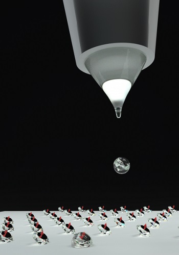
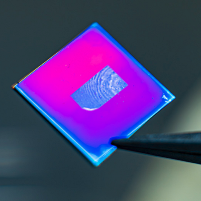
Nano-precision printing of NV-center nanodiamonds using the new technology.
The team led by Dr. Ji Tae Kim from the Department of Mechanical Engineering and Dr. Zhiqin Chu from the Electrical and Electronic Engineering of the University of Hong Kong (HKU) has developed a nano-precision printing method for nitrogen-vacancy (NV) centers in diamond at the quantum level, meeting the technological requirements.
This novel approach is practical and cost-effective, paving the way for manufacturing of quantum information processing device, quantum computing and biosensing devices.
The research achievement has been published in Advanced Science in an article titled “On-Demand, Direct Printing of Nanodiamonds at the Quantum Level”, and featured as a Back Cover story by the Journal. A US patent has been filed for the invention.
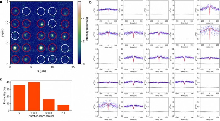
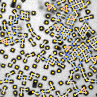
Printed NV centers at the quantum-level. a) Confocal fluorescence image. b) Second-order correlation functions g(2)(τ) of corresponding fluorescence spots. c) Number distribution histogram of printed NV centers per spot.
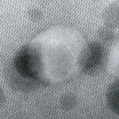
The NV center is a point-defect in the diamond lattice and is the most common defect in nanodiamonds. It has emerged as a powerhouse for quantum systems due to their robust quantum states even at room temperature while other quantum systems such as superconducting quantum interference device can only operate at cryogenic temperatures, i.e., from −150 °C (−238 °F) to absolute zero (−273 °C or −460 °F).
Specifically, this atom-like solid-state device with its optically addressable spin-degrees-of-freedom, provides the key functionalities for serving as the quantum bit and/or quantum sensor in solid-state quantum processors.
“Diamond is the hardest material, so it is difficult to craft”
The researchers have developed an innovative way to tackle this issue. They have utilised electrical dispensing of nanodiamond-laden liquid droplets with sub-attoliter (< 10−18 liter) volume for placing NV-centers directly on universal substrates.
“To the best of our knowledge, the developed technique, for the first time, shows sub-wavelength positional accuracy, single-defect-level quantity control, and freeform patterning capabilities, meeting the technological requirements which marks a significant breakthrough in quantum device manufacturing,” said Dr Chu Zhiqin.
Read the original article on The University of Hong Kong.