The third dimension may be responsible for preventing electronics from becoming thinner, tinier and more flexible, according to an international collaboration that developed a way to manufacture new, idealized two-dimensional semiconductor materials. They published their approach on June 3 in Nano Research.
The researchers, led by Lin Zhou, associate professor of chemistry at Shanghai Jiao Tong University in China, focused on indium arsenide (InAs), a narrow bandgap semiconductor with properties useful for high-speed electronics and highly sensitive infrared photodetectors. Unlike most of the existing 2D materials with layered strucutures, the problem, Zhou said, is that InAs typically has a 3D lattice structure, which makes it challenging to transform into ultrathin 2D films for advanced electronic and optoelectronic applications.
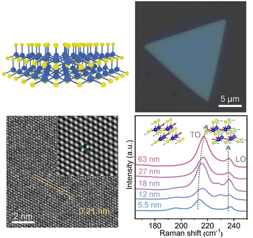
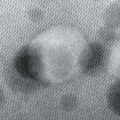
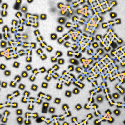
Researchers obtained high-quality 2D InAs single crystals via van der Waals epitaxy and explored the optical and electrical properties of InAs single crystals.
“The growth of large, ultrathin 2D non-layered materials has been a grand challenge, but one worth solving.Thanks to its high mobility and tunable bandgap, 2D InAs could be a critical material for next-generation, high-performance nano-electronics, nano-photonics and quantum devices,” Zhou said. “It has the advantages of both InAs, such as high carrier mobility, small and direct bandgap size, and 2D materials, which have an ultrathin nature suitable for small size devices, are flexible and transparent.” This work also provides a promising way to further expand the group of 2D semiconductors by incorporating materials with non-layered structures.
The researchers took advantage of a weak atomic attraction known as the van der Waals force in epitaxy growth. The force describes how neutral molecules can connect with one another, while epitaxy involves applying an overlay of one material to a crystal-like substrate. Using atomically flat mica, which is naturally layered, as a substrate, the researchers grew a thin layer of InAs. The molecules in the mica substrate and the molecules in the InAs are mutually attracted enough to connect, preventing the InAs from growing into a 3D lattice. Moreover, the van der Waals growth ensures strain-free and no misfit dislocations in as-grown 2D InAs. The InAs can be incredibly thin with desired properties.
Zhou also noted that the InAs and the substrate do not covalently bond, so they can be separated and the substrate re-used, making the synthesis process more cost-effective.
“We also found that we can tune the properties of 2D InAs by changing the material’s thickness due to the quantum confinement effect,” Zhou said. “The 2D InAs is easy to tailor to achieve desired properties and to integrate with other compounds. In addition to manipulating the thickness during synthesis, we can also stack 2D InAs with other 2D materials to form heterojunctions for multifunction performance, giving them significant advantages in electronics and photovoltaics.”
The final 2D InAs material takes the form of triangular flakes, roughly five nanometers thick. That’s about 0.0007 the size of a single red blood cell. The tinier the material, the smaller the devices it will eventually comprise, Zhou said.
“Prior to this work, high-quality 2D — meaning less than 10 nanometers thick — InAs had not been reported, let alone a scalable synthesis of 2D InAs single crystals with unique optical and electronic properties,” Zhou said. “Our work paves the way for miniaturization InAs-based devices and integrations.”
Next, Zhou said the team will explore new 2D semiconductor to grow with an ultimate goal of achieving scalable synthesis of high-quality 2D materials over large areas for multi-functional applications.
Read the original article on Eurekalert.