We view the world through visible light wavelengths on the electromagnetic spectrum, ranging from 400 nanometers to 700 nanometers. Other segments of the spectrum — measured in meters based on the distance between the crests of oscillating waves — serve different purposes. For example, some wavelengths on the electromagnetic spectrum smaller than visible light are used in X-rays. Other segments of wavelengths larger than visible light are used for radio and microwave ovens.
Advances in technology to make better use of the infrared radiation spectrum — or the electromagnetic waves that are just larger than visible light — hold the key to improving optical modulation, a process that uses light to transmit data through patterned pulses.
Yu Yao, an associate professor of electrical engineering in the Ira A. Fulton Schools of Engineering at Arizona State University, and her research team at the ASU Center for Photonics Innovation have developed a graphene-metal hybrid material to achieve ultrafast optical modulation.
The work represents the world’s first demonstration of ultrafast optical modulation at mid-infrared wavelengths using the graphene-metal hybrid material. Results of the research, conducted with Fulton Schools graduate researchers Ali Basiri, Md Zubair Ebne Rafique, Jing Bai and Shinhyuk Choi, were recently published in Light: Science & Applications, a Nature journal.
“Our specific design targets light with a longer wavelength for which it is challenging to achieve optical modulation using conventional materials and devices,” Yao says. “We can achieve unprecedented, very strong modulation of an optical signal in a very short amount of time: one trillionth of a second.”
The group’s design will enable new or improved applications in satellite communications and ultrafast molecular spectroscopy to study chemicals and molecules and advance biomedical diagnostics, remote sensing and astronomical applications — for example, in research being conducted on-site on the moon or Mars.
Optical modulation and the electromagnetic spectrum
Optical modulation involves two laser beams of light called pulses: the pump pulse and the probe pulse. How these pulses are used depends on the application.
In communications applications of optical modulation, the pump pulse is a steady beam of light. The pump pulse gets modulated to emit a probe pulse, which carries the information that can be decoded back into data by a receiving device. For instance, fiber optic internet connections, which are among the fastest types of internet services, use optical modulation through glass or plastic fibers to transmit data.
Spectroscopy applications measure information about a substance based on how materials interact with different wavelengths. In these cases of optical modulation, the pump pulse excites, or vibrates, the molecules in a material, such as a new drug or another chemical. The pump pulse is then followed by the probe pulse, which passes through the material and relays information about it to a detector.
The wavelength from the pulses at which optimal modulation is achieved is also important because of how matter and electromagnetic radiation interact at various wavelengths.
The wavelength of visible light, for example, is easily blocked or scattered by dust and other particulates in outer space and is therefore ill-suited for long-distance communications applications of optical modulation. In the infrared spectrum, waves can travel farther with much less scattering, so scientists are working on achieving optical modulation at these wavelengths.
The mid-infrared spectrum Yao’s team is exploring has waves that range in size from about 6 micrometers to 20 micrometers, a measurement also called a micron (25,400 microns can fit in 1 inch). It is also the range at which many materials vibrate, so there are potentially many more materials that can be explored through spectroscopy. But first, the team would need to develop an effective mid-infrared optical modulation device
New material combination opens up the future of optical modulation
Yao’s research team created a device that produces and interacts with the probe pulse, using a unique combination of materials that enable optical modulation at larger wavelengths than what has ever been possible.
Previously, researchers have used silicon and other materials to create these kinds of devices. However, they are too bulky and absorb too much of the target electromagnetic waves to be effective at the larger infrared spectrum, beyond 5-micron or 6-micron wavelengths.
The team’s design incorporates an ultrathin, single-molecule layer of graphene with an artificially engineered metal to form the hybrid material that was used for the first time for ultrafast optical modulation.
“We identified materials that can interact with a broad wavelength wave, and graphene is one of them,” Yao says. “Graphene is very thin; fabrication is very easy, and we can do the fabrication and transfer the graphene onto anything. We understand that because it’s such a thin layer, the interaction with light is strong and can be enhanced.”
The light interaction is enhanced through the use of a tiny cavity in the graphene hybrid material device, which interacts with the engineered material to achieve a stronger optical modulation effect than other designs.
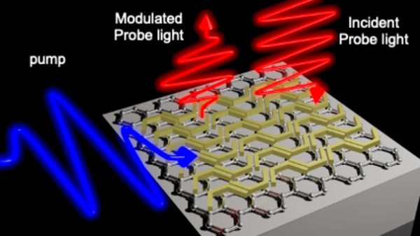
An illustration of the device with the pump light (blue line) and incoming incident probe light (right red line). These lights are focused onto “nanoscale hot spot” gaps in the graphene layer (hexagons) between antennas (shown in gold) on the device. A modulated probe light (center red line) is the result of optical modulation.
Applications near and far
The optical modulation at larger wavelengths that Yao’s device makes possible will allow signals to travel farther, enabling better long-distance communication between satellites in space, or even between satellites and Earth.
“Visible light can only go so far because it’s highly scattered by dust and everything else in space,” Yao says. “But with the longer (mid-infrared) wavelength, the scattering effect is much less and (the signals) can propagate much farther.”
This design will also improve efficiency in other applications, including remote sensing, which can use the mid-infrared spectrum pulses to determine the composition of distant objects, such as a plume of smoke.
The semiconductor industry can take advantage of Yao’s team’s tiny device to enable silicon technology to work for communications with satellites and vehicles in outer space. Due to their super compact size, devices like the one Yao’s team has demonstrated can be included directly on integrated circuits.
"To realize compact system solutions, it’s always desirable to develop optical modulators that can be directly integrated on silicon, and it is possible for our device,” Yao says.
The technology can also be used to characterize new materials and understand how they can be implemented to achieve advances in semiconductors.
Aiming for bigger and better
So far, Yao’s team has demonstrated a critical next step beyond 6-micron wavelengths, showing a strong optical modulation at 6 microns to 7 microns.
“We’re targeting even longer wavelengths because we know that 8 to 12 microns is a window that can pass through the atmosphere with the least scattering,” Yao says. “But we have to take it step by step.”
Read the original article on Arizona State University.