Rob, what background information will help us understand where Nantero is today in its profitability quest?
I’m the CEO and have been since August 2021. That’s when the company was purchased by the Overview family, who have been involved in the semiconductor business for years through one of their construction businesses focused on contracts to build secure microelectronics facilities.
I’d been running one of their other investments through a company called Honeycomb. This was a company established to commercialize several carbon nanotube (CNT) microelectronic technologies developed by the U.S. government that no longer needed to be classified. In trying to execute on the mission of Honeycomb, all CNT–related roads led back to Nantero and the very mature CNT process flow and fab–stable aqueous CNT solution they’d developed, as well as the non–volatile carbon nanotube memory, NRAM, they’d invented.
I’m a former Navy SEAL, having served two tours in Iraq. I received my MBA from Wharton, where I got my start in Silicon Valley with a startup called Project NMSET. We developed a MEMS technology that could be useful as a microscale propulsion device, but it had issues operating at sea level. We found some interest for the technology at NASA Ames Research Center, to be used for Martian rover projects. But we pivoted it to become a medical device. That technology is now going through FDA trials.
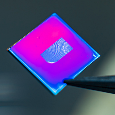
Nantero is the world leader in CNT semiconductor technology and has been developing both non–volatile memory and, most recently, CNT–based transistors. The Overview family’s vision for the company has been to transition it from a licensing–focused company to a product company. The company has been around for 20 years. For the first 10 years, Nantero was essentially a chemical company that was developing CNT solutions to go into spin coaters and semiconductor fabs. Nantero has done some very impressive chemical engineering and has come up with a very particular process to spread carbon nanotubes uniformly across a 12–inch wafer that can be accepted in high–quality fabs.
Over the past seven years, there was a transition within Nantero to focus on building devices out of this fab–stable CNT process. That’s been a real challenge as a startup company; to prove your technology in a commercial setting is extremely expensive and cost prohibitive. There wasn’t enough time within any one engagement to mature the technology within a high–quality, commercial–scale fab so that it could merge into the commercial roadmaps established by partners who were interested in our memory. At least one of the engagements was to get NRAM onto a DIMM card, which means you’re going up against a perfected memory cell like DRAM that’s been around for 60 years; it’s difficult to compete on the purity and the perfection of the memory cell itself, but that’s what Nantero was going for.
In that particular engagement, at a two–sigma level, our bits were operating exactly as Nantero had expected, which was as a non–volatile, high–performance potential DRAM replacement. But we weren’t going to get there within the amount of time we were allotted within the fab to eliminate those troublesome tail bits so that we could talk directly to the processor and merge with the commercial roadmap. The project was scuttled. Nantero has improved this number, and we have now achieved five-sigma quality through our most recent, and ongoing, engagement with Fujistu. We now have enough information to build what we know we can do and we’re going to do it on our own scale, and in our own timeline, because we know that the prior engagements with the big guys ran up against a global shortage of fab space. Also, CXL architecture is opening a great door and we’re very excited about that.
There is great interest in our technology. We’re making some great progress with our Japanese partners who have invested and are betting heavily that CNT semiconductors will be a huge growth industry. They have helped us establish a project funded by the Japanese government. We’re the only memory technology chosen inside their Green Data Center Initiative, and a $100 million funding pool has been established to further develop our CNT NRAM technology.
We aren’t the direct beneficiaries of that money as we’re not a Japanese company. But many of our Japanese partners who joined the consortium will be. This is a great thing for the advancement of our technology and those that believe in it, but not such a great thing for Nantero or for keeping this technology in the U.S.
The CHIPS Act is important because, for the first time ever, we might see this level of investment possible from the U.S. side.
Anyone who has tried to launch a breakthrough semiconductor technology will tell you: small sources of state–backed capital aren’t enough to keep a U.S. technology at home. We came out of the Harvard School of Chemistry, where Nantero co-founder and CTO Thomas Rueckes invented the technology. It wouldn’t be unusual to see our technology lost overseas even though it came from an elite U.S. research institution. That’s where the capital has traditionally existed to overcome the infamous “Valley of Death” that plagues virtually all U.S. startups in this industry.
I applaud and thank the Biden administration and this congress for their bipartisan effort because while it’s very complex and perhaps not easily understood, it’s vitally important to the U.S. economy and will help to retain trillions of dollars of economic expansion and national security interests over the short and long term.
I recently interviewed Keith Krach. He was the undersecretary of state in the Trump administration and a key architect of the CHIPS Act. (CHIPS stands for “Creating Helpful Incentives to Produce Semiconductors,” but the act goes beyond computer components.) Krach was saying we’ve got to find a way to keep technology developed in the United States from going overseas. And he was saying in particular, China. I don’t think that’s really a danger in Nantero’s case. Right?
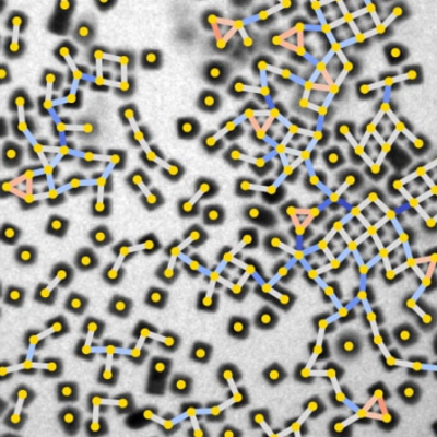
Carbon nanotubes are one of the few natural semiconductor elements in existence. Several companies, including most famously IBM, had CNT programs but have given up. People who write us off say, “if IBM couldn’t figure it out, then you guys certainly can’t.” We’re doing something completely different than what they did. As I understand it, they were trying to align individual tubes or at least make specific directional alignments of tubes that was just too hard. We find conductive pathways through a mesh of tubes within an aqueous slurry that’s spread out over the wafer, and we have proven that. Several companies have been very impressed with what we’re doing, and we hope to announce some of our significant strategic engagements coming up.
In regard your question about China, you’ll find CNTs on corporate roadmaps usually for transistors. It’s largely understood that CNTs will offer the best opportunity to create a perfectly linear transistor, but ultimately everybody thinks that’s 10 years down the line. That would be somewhat of a “holy grail” for transistors. Here’s the interesting thing, however. Our thin–film CNTs spread out uniformly over a 12–inch wafer, and we have perfected that process to create a very beautiful blue coating that we’re now using to build transistors. We have a program with Purdue University, under Joerg Appenzeller, where we’re building transistors. Purdue has been a really great partner, and we’re very appreciative of their leadership. CNT transistors may not be so far away as everyone thinks.
Analog Devices and SkyWater have been working with MIT to commercialize carbon nanotube technology. How do these companies stack up?
From what I have heard, we’re far in advance of where they are. From my year with Nantero, I have been unbelievably impressed. Nantero has already solved many of the issues they are running into with the work at MIT. It’s my assessment that Nantero has an “embarrassment of riches” with what it has accomplished in fab.
At this point, how has Nantero commercialized CNTs?
Nantero is engaged with Fujitsu on a milestone–based performance program for a chip that would ultimately lead to licensing revenue for Nantero. While our company focus is now to build our own chips and get away from licensing, we’re honoring this prior commitment. Five years of uninterrupted development within a high–quality fab has given us extremely important data. Fujitsu has advertised that our technology is aimed to merge within their ferroelectric business line.
This project was supposed to have been delivered in 2019. This was a problem with the licensing business previously held by Nantero, as they had financial difficulty in meeting the R&D spend necessary to hit the milestones as defined by Fujitsu. When I came in as CEO, we started funding the development again and are back on target with an extended timeline.
The U.S. government has employed the use of NRAM for several applications, especially in space. Lockheed Martin purchased the rights from Nantero to pursue government business a long time ago, and so I am not certain of all the applications, but I do know from my work with Honeycomb that NRAM has had success within these small–batch applications.
Nantero has had working chips for decades. Filling small batch requests from Lockheed or anyone else hasn’t been a problem; we can easily find working parts on a wafer and fill orders for niche applications. The real challenge for a commercial memory company is getting six-sigma yield. If you must throw away 20% of your chips (not including edge chips), you aren’t going to be competitive.
The new company focus is building what we know we can do. We know exactly the heartbeat of NRAM, what it’s capable of, what we need to do with a controller outside the memory cell. We’re going to push that into the marketplace.
How soon is that going to happen?
We have an engagement. We have a foundry lined up. We haven’t signed documents just yet as the CHIPS Act possibilities aren’t decided, and those dynamics could drastically change any business agreement. We also have base wafer commitments coming from one of the big foundries in the U.S. We have aligned a program that will have us to market with our own competitive CNT memory chip in 24 months.
Is Nantero profitable? It’s not public. So, it’s kind of hard to see the financial information, all that sort of stuff.
Nantero isn’t profitable. It’s made about $130 million during its 20–year existence. We’re an R&D company in transition to a new business plan. We spend a lot of money in those valleys between when you make money and when you come out with your next chip. That doesn’t mean that Nantero hasn’t been profitable in the past, but since we have been refocusing the business model, it’s not.
Do you have any insight into when the company might become profitable?
Nantero has sold chips in the past. With the Fujitsu engagement, we’re essentially paying for the development of the chip they want, and at certain milestones they will start paying us licensing revenue. That would be enough to make Nantero profitable. But we can also focus that chip for applications outside of Fujitsu’s interests, and that’s the nearest term target that we have; we can take the chip that’s already at a five–sigma level and work toward commercialization. We can be profitable within six months based on revenue from this activity. It’s not going to be the DRAM–level, CXL–polished chip that we’re planning to build in 24 months, but it will be a nonvolatile memory for niche applications.
Just to recap a bit, your first products would go on DIMM cards, right? And then CXL?
We have a ton of data from our last engagement on what would be a DIMM card. That would be the “holy grail” of memory. We can continue to build toward that end and to getting errors corrected on chip, but in conjunction, we can go after a system–level solution in CXL architecture.
The chip we’re planning to build will present as a DDR5 chip, and CXL is a very attractive way to make that happen. When it comes to those tail bits, you can do off–chip error correction within the CXL module itself. That would allow the excellent performance and added features of NRAM to be deployed while we continually enhance the cell itself, and one day can perform directly on the DIMM bus.
NRAM is the fastest reading memory, with reads between 2 and 20 nanoseconds depending on the cell architecture; if you put a system wrapper around that to bump up our write times, we’re still faster than the others. We can put a system wrapper around it that preserves that super low latency starting point our technology offers. From there, we will start to get to next generations of the core cell design, and we will begin to build toward that excellent performance that DRAM has developed over its 60 years of deployment. CXL will accelerate all of that.
Would the plan be to license technology at the same time as you do manufacturing?
We have transitioned the company from a licensing focus to a product focus. The Fujitsu project was so far along that we decided to continue with the current plan for that specific product, even though it’s a licensing arrangement. When we achieve the milestones set out in that engagement, hopefully they would still be interested to take the chip in–house and pay the licensing fees, or maybe they will simply choose to buy it from us.
You are expecting to find a foundry partner?
Yes, Nantero is fabless. We have our chemical facility in Woburn, Massachusetts, where we can get from raw material to fully completed CNT spin coat layers on a 300–mm wafer. The wafers go to fab wherever our current engagement is at the time. Finally, the wafers are either sent back to us directly after passivation, or they’re diced and packaged before they come back. But either way, they go to our Sunnyvale, California, facility where we have Maverick testing machines.
We completely outsource our foundry work, and naturally, most of that’s overseas. We do, however, need a fab for consistent development of the technology. Through the Fujitsu project, we were last in the UMC (United Microelectronics) fab in Mie, Japan, which is called USJC. That was the last foundry we were in through December of 2021. Now, we have a new engagement set up here in the U.S.
Now that the CHIPS Act has passed, we’re anticipating the landscape for emerging technologies to get better. Not all emerging technologies will work out. Companies either go overseas where there’s capital to make it across the “valley of death” or they simply go away, and the technology gets purchased for very cheap by a larger company.
With regard to the CHIPS Act, you said it’s possible that Japan will take the lead in this business. Why would that matter?
The policy makers and ultimately President Biden —who signed this bill into law yesterday— understand that we’re not going to recreate what’s already been created in Taiwan or Shenzhen or wherever. What they have said specifically in the language of the bill is that the CHIPS Act is about “breakthrough technologies,” as well as manufacturing capability in the United States. We have to find breakthrough technologies to get back into the race, and the U.S. happens to be the birthplace of many of the world’s best technologies. They just haven’t been able to stick around to benefit the U.S. economy as the capital has been overseas.
Not all $52 billion is about funding breakthrough technology companies and research. The largest portion of the funding, I believe about $32 billion, is going toward returning manufacturing capability to the U.S., and that’s extremely important. However, Provision 9906 of the bill would establish the National Semiconductor Technology Center (NSTC) for about $10 billion, and that will help breakthrough technologies that are struggling to stay in the U.S. There is, of course, a risk that highly profitable companies will simply try to leverage the NSTC to fund their own corporate R&D projects that would have been funded out of corporate profit.
Congress, President Biden, and U.S. commerce secretary Gina Raimundo have done an excellent job in setting up the industry for success where larger companies will lead the way. But smaller companies won’t be left out in the cold. I am confident the larger companies will see that they will be more successful if they work with us. The end result will be that this investment of $52 billion by the taxpayers will return 50–100x.
Our technology will be inexpensive to produce and will help to significantly reduce the energy needed to run servers and datacenters.
NRAM doesn’t require refresh or pre–charge, and can reduce energy consumption by 30% overall in these systems. The energy savings are like replacing incandescent light bulbs with LEDs, and this is why the Japanese have included our technology into their plan to make Japan carbon neutral. We think this is a wonderful initiative, and we’re proud to be a part of it. We just hope that the U.S. will recognize that the memory technology to help achieve this goal is here at home and support a U.S. program with similar goals.
The Japanese project is called the Green Innovation Fund, and they have established ¥2 trillion yen ($14.8 billion) for the program aimed at making Japan carbon neutral by 2050. Within the larger program, there’s the Green Data Center initiative, worth about $1 billion. That’s where Nantero’s CNT memory has been picked as the only memory technology included in the program to offer solutions for a more energy efficient datacenter model. The program has established $100 million for Japanese companies to further develop NRAM. An investment of at least this size from the CHIPS Act will help keep the technology onshore where we invented it.
There are competing technologies like MRAM. How do you think NRAM stacks up?
Number one, as I understand it, is that we’re way cheaper; MRAM uses some very expensive materials. The major success that they have had has been as a non–volatile memory technology offered by fabs within chiplet designs and embedded memory into or next to logic devices. For this reason, a customer may be willing to pay the extra cost for MRAM as a non–volatile memory solution, because there’s just not much of it that they would need to buy.
MRAM would have a hard time commercializing as a standalone memory or in storage–class memory applications. Several big companies have taken MRAM seriously because it’s a great technology.
Nantero hasn’t focused on embedded applications yet, but we certainly should. When we do, we will be able to compete very well on cost with MRAM. MRAM is used in space applications, but there are some issues with magnetic fields. Our NRAM is immune to these issues, and when we were launched on a mission aboard space shuttle Atlantis in 2009, we performed for the duration with zero soft errors. We’re immune to disruptions by magnetic fields, and perhaps very relevant to today, we’re completely radiation hardened.
Many of the other emerging memories in the “emerging memory zoo,” as it’s called, have gone the system–correction direction already. Nantero has been trying to compete with DRAM for many years and throughout many engagements. Designers of other emerging memory technologies, by comparison, have accepted the imperfect nature of their cell design and chosen to correct their errors off–chip with a controller. I am excited to see what amazing performance characteristics we can pull through an off-chip correction process.
Do you think that Nantero is going to win in any of this CHIPS Act money?
I do. We have demonstrated that our technology is legitimate and has real potential to lower power consumption by 30% in data centers as well as offer new capabilities to next–generation computing processes. We’re the only American–based emerging memory company that’s 100% American owned, and when it comes to addressing the issue of secure supply chains, Nantero offers a really good solution. Nantero–sized chip projects are $100 million to $200 million based on where we are in our technology life cycle.
Private investors have committed to make private contributions to a CHIPS project secured by Nantero, and we also have state governments that are interested to have this work come to their states. You can create an industry around it, you can create jobs around it, and you can create national defense initiatives around it, and that’s what other countries have realized for so long. The U.S. government has now made the great decision of getting into that game and competing. The U.S. has the best research universities and institutions in the world, but loses the economic benefits of commercialization overseas far too often. If we’re so fortunate to get an award, we understand that taxpayers expect performance out of us.
Read the original article on EE Times.