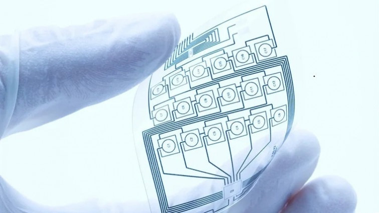
“Flexible and transparent electronics is typically associated with wearable biosensors that monitor vital signs, such as heart rate, breathing, and blood oxygenation, and relay them to a smartphone or fitness band,” Skoltech PhD student Aleksei Shiverskii, one of the inventors, comments. “An affordable and efficient technology that at first may seem impractical soon becomes a ubiquitous and indispensable appliance, like a bluetooth electric kettle or a wifi vacuum cleaner. I believe that someday flexible and transparent electronics will become a fixture, too.”
Currently, metallic meshes embedded in polymer or glass are used as conductors in flexible transparent electronics. The most common metals for a mesh are copper, silver, and even gold or platinum for hi-end devices. However, the metallic meshes that heat the glass can hardly be called transparent. Although they cope quite well with their task, the finest mesh only lets through about two-thirds of the light. As opposed to metallic meshes that you can see with a naked eye, graphene is more transparent, less visible, and highly conductive. Besides, some studies show that graphene has higher bending fatigue strength and, therefore, can last longer.
Importantly, graphene is made from much cheaper and eco-friendlier materials as compared to pure metals and, unlike copper or silver, is not susceptible to oxidation.
Typically, graphene is synthesized on a temporary substrate and then transferred onto a permanent polymer substrate that supports and shapes it as needed. The transfer is performed using the poorly scalable Langmuir-Blodgett method that tends to cause defects and impair the quality of graphene. The Skoltech team has come up with an alternative solution to deal with the transfer issue that prevents widespread adoption of graphene in flexible transparent electronics.
“Graphene is usually produced using a temporary flat substrate. In the Langmuir-Blodgett method, the substrate is dissolved once the synthesis is complete, with graphene film left floating on the liquid surface. Then a permanent substrate is slipped under the film for graphene to take the required shape. It is at this point that defects appear in the material,” Shiverskii explains.
“In our method, the temporary substrate is made to match the ultimately desired graphene shape. Once we have placed the permanent substrate onto the film, we remove the temporary one. Since graphene settles down in its final shape, there is no need to drape it over the permanent substrate, which helps avoid wrinkles and other defects. The 3D temporary substrate offers much broader possibilities than conventional techniques. Now, along with 2D or quasi-2D circuits we can produce 3D circuits of whatever complexity we wish with a resolution of several dozen nanometers,” patent co-holder and Skoltech Assistant Professor Sergey Abaimov says.
He continues, “The patent discloses a specific optimal lab-tested method, in which we create a photopolymer mask with the shape of the future graphene structure on a catalytic copper substrate, coat it with chromium, and then remove the polymer, leaving a negative chromium mask of the required shape on the substrate. We use chromium because it withstands high-temperature synthesis and passivates graphene in covered areas. Along with this method, the patent presented more general approaches — both in the description and formula — covering a broad range of alternative methods.”
“I expected multiple revisions of this complex patent but to my surprise, the application was approved right away, with only minor technical corrections. I hope that our research will have wide application and help propel Russian technology in flexible and transparent electronics to new heights,” Abaimov concludes.
Read the original article on Skolkovo Institute of Science and Technology (Skoltech).