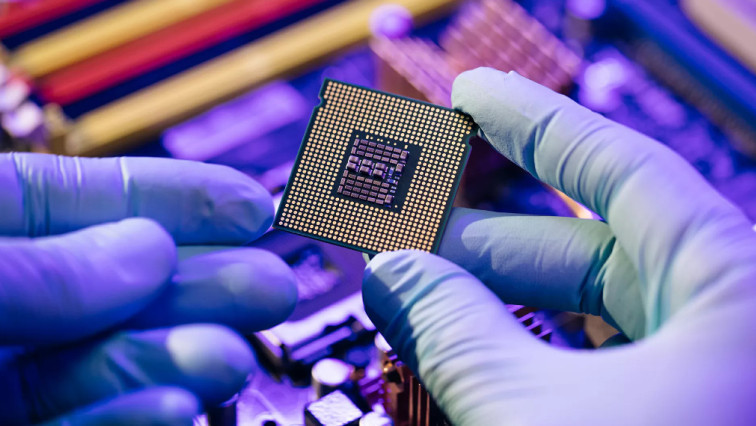
At the heart of every mobile phone, laptop and autonomous vehicle is a tiny semiconductor whose properties and, ultimately, performance are determined by free electrons. Now, UC Berkeley researchers have developed a new way to measure these electrons that could lead to more energy-efficient semiconductor materials and electronics.

Optical nanoscopy uses laser beams to strike free electrons, scattering light and providing insights into electron distribution and dynamics within semiconductor materials.
As reported in Nano Letters, researchers demonstrated a new type of optical nanoscopy that can measure electron dynamics in semiconductors, a task that has become more challenging as demand grows for ever-smaller and faster integrated circuits. With the components of many everyday electronic devices already at nanoscale, new tools are needed to measure electrons with high resolution.
“Our optical nanoscopy integrates near-field scanning optical microscopy and pump-probe optics to enable high resolution at both spatial and temporal scales,” said Costas Grigoropoulos, professor of mechanical engineering and principal investigator of the study. “And this technology can be applied to a wide range of semiconductor materials, including silicon, germanium and gallium arsenide as well as other exotic materials, such as 2D materials and ferroelectrics.”
In other words, the optical nanoscopy tool uses a combination of optical imaging and laser probing technologies to measure electrons, or energy carriers, at picosecond and nanometer scales. These measurements may offer insights into how energy carriers are distributed and the way they behave within semiconductor materials, which can impact energy efficiency and other properties.
According to Jingang Li, lead author and a postdoctoral researcher in Grigoropoulos’s Laser Thermal Lab, this research represents an important step toward investigating and further optimizing energy savings for semiconductor-based electronic devices — such as mobile phones, LEDs, industrial solar cells and sensors.
“With a high density of chips in integrated circuits, the electron distribution and transport not only control the device functionality, but also govern the heat generation and dissipation process,” said Li. “Our nanoscopy will enable the investigation of nanoscale thermal management in these densely packed devices.”
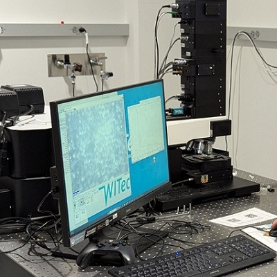
To measure the electrons in a semiconductor, optical nanoscopy employs ultrafast lasers and an atomic force microscope (AFM) tip with an apex curvature of less than 30 nanometers. Researchers shine two laser beams — a pump beam and then a probe beam — onto the AFM tip. The first beam excites electrons in the sample, and after a carefully timed delay, the second beam strikes the tip. Then, the local information on electron properties can be obtained by analyzing the scattered light of the second beam.
Li thinks that optical nanoscopy may have applications beyond measuring electrons in semiconductor materials. “Because it’s a versatile optical diagnostic tool, it can be used to study many other physical phenomena and functional devices, such as phase transitions and data storage,” he said.
Read the original article on University of California, Berkeley.


