Researchers have developed an easy-to-build, low-cost 3D nanoprinting system that can create arbitrary 3D structures with extremely fine features. The new 3D nanoprinting technique is precise enough to print metamaterials as well as a variety of optical devices and components such as microlenses, micro-optical devices and metamaterials.
“Our system uses a two-step absorption process to realize 3D printing with accuracy reaching the nanometer level, which is suitable for commercial manufacturing,” said research team leader Cuifang Kuang from the Zhejiang Lab and Zhejiang University, both in China. “It can be used for a variety of applications such as printing micro or nanostructures for studying biological cells or fabricating the specialized optical waveguides used for virtual and augmented reality devices.”
Conventional high-resolution 3D nanoprinting approaches use pulsed femtosecond lasers that cost tens of thousands of dollars. In the Optica Publishing Group journal Optics Letters, Kuang and colleagues describe their new system based on an integrated fiber-coupled continuous-wave laser diode that is not only inexpensive but also easy to operate.
“This new approach helps make 3D nanoprinting accessible to scientists, even ones who are not familiar with the optical systems typically used for this type of fabrication,” said Kuang. “It could eventually lead to low-cost desktop 3D nanoprinting devices that could offer precision nanoprinting to anyone.”
Creating a simple setup
3D printing objects with a feature size of approximately 100 nm typically requires a technique called two-photon absorption. This involves using expensive femtosecond lasers to achieve precision 3D photon absorption that solidifies, or polymerizes, a liquid resin that is sensitive to light.
Recently, an approach called two-step absorption has been developed as an alternative to two-photon absorption developed by Vincent Hahn’s research team at Karlsruhe Institute of Technology. It uses a special photoinitiator called benzil together with a single light source to create polymerization. In the new work, the researchers developed a simplified and faster 3D nanoprinting two-step absorption system that uses a 405-nm-wavelength integrated fiber-coupled laser.
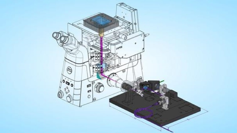
For 2D or 3D printing with the new system, the laser beam from the single-mode polarization-maintaining fiber is collimated and directed onto galvanometric mirrors. It is then focused into the photosensitive material with a high-numerical aperture microscope objective.
Printing tiny objects
“The simple system does not need a large number of optical components to modulate the laser beam, which saves money and produces less optical aberrations, or errors,” said Kuang. “It is also highly stable and compatible with most commercial microscopes.”
The researchers demonstrate their 3D nanoprinting system by using it at low speeds to print 2D line gratings and 3D woodpile nanostructures with a lateral period of 350 nm. Using a faster scan speed of 1000 micron per second, 2D gratings with sub-200-nm resolution and sub-50-nm linewidth can still be fabricated with laser power less than 1mW.
The researchers are now working to improve the writing speed and quality of the technique while maintaining high resolution. This will make the system practical to use for even more applications.
Read the original article on Optica.


