If you’ve read any stories about quantum research lately, in Columbia News or elsewhere, you may have heard the term 2D, or two-dimensional, materials.
In January, Columbia chemists published a study about the first 2D heavy fermion, a class of material with very heavy electrons. In November, the Engineering school published a story on “Laser-Driving a 2D Material.” And earlier last year, researchers found both superconductivity and ferroelectricity in the same 2D material. The list goes on.
So, what are 2D materials and why are scientists so interested in them?
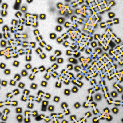
Two-dimensional materials are just what they sound like: Materials that are just 1 or 2 atoms thick, but wider in every other direction. Often the 2D materials scientists are working with are a few square micrometers large– invisible to the naked eye, but visible with the kind of microscope you might have used in high school science classes.
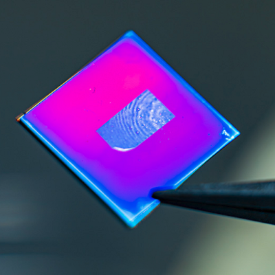
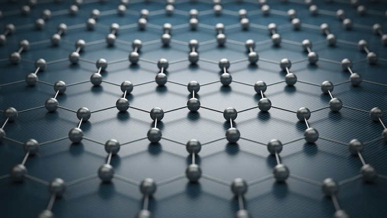
The 2D materials that scientists are working with are a mix of naturally occurring materials, like graphene, a form of ultra-strong carbon discovered at Columbia in 2004, and materials synthesized in labs, like CeSil, a crystal first assembled at Columbia last year, composed of cerium, silicon, and iodine.
These materials usually begin as three dimensional, and scientists peel them down to two dimensions to run experiments on them and find out what physical properties, like superconductivity or magnetism, might emerge when the materials are atom-flat. Scientists are working on developing new ways to make 2D materials from scratch, without needing to peel them down from 3D, but the quality of these is still imperfect.
Many things make 2D materials interesting but a primary one is that they confine the ways that particles like electrons can move within them. Columbia Chemist Xavier Roy used a traffic analogy to explain:
“Think of it like this: If we had flying cars that could travel in three-dimensional space, we would be able to reduce most of the traffic in New York. But since our current cars can only travel in two-dimensions, we end up with huge traffic jams in Times Square,” Roy said in a recent interview.
“The same thing happens for electrons when we move from 3D to 2D, but in our case, ‘traffic’ between electrons is beneficial! As these electron-electron interactions become stronger, we can completely change the properties of a material. For example, as the thickness of 3D heavy fermion materials is reduced (i.e. as they become more 2D), they can transition from being magnetic to superconducting.”
Two-dimensional materials can also be relatively easily tweaked: Stacking them with slight angles between the layers, applying forces like electric fields and magnetic fields, and straining the materials by twisting or applying pressure to them can change their properties. Take just one example: By simply stacking two sheets of a material called tungsten diselenide on top of each other, twisting them, and adding or removing electric charge, the material can switch from an electricity-conducting metal to an electricity-blocking insulator and back again.
Scientists are also excited by 2D materials’ potential uses in technology, which scientists often refer to as “applications.”
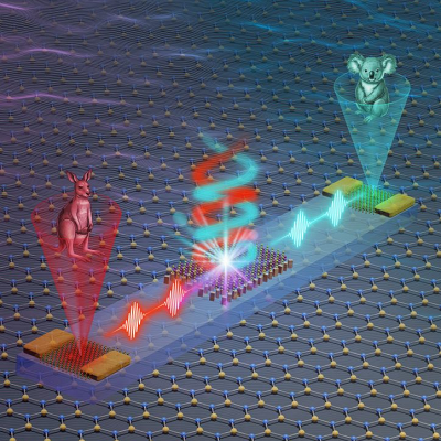
Two-dimensional materials will likely play a vital role in the next generation of electronics, including still-under-development quantum computers. Why? In large part, because 2D materials are ultra-small with unique, controllable properties (like superconductivity), and technology is always on the hunt for something that can achieve results more quickly, more efficiently, and using less space.
Read the original article on Columbia University in the City of New York.