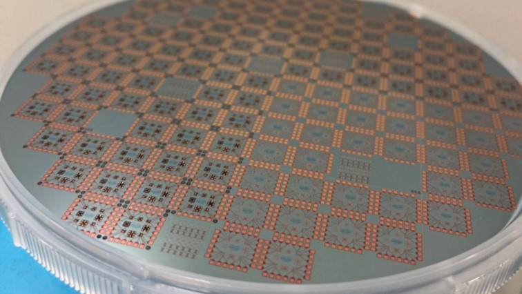
Archer sent the Biochip gFET design to Graphenea for fabrication through a whole wafer run in December 2023.
According to the company the gFETs are designed with structures suitable for liquid multiplexing, with advances in chip design features, including in gating design and materials, to address technological challenges in maintaining graphene device stability from chip-to-chip.
The process run was performed on a six-inch whole wafer producing 145 chips with eight gFET devices on each chip, making it the first six-inch wafer run for Archer.
The CEO of Archer Dr Mohammad Choucair said: “Archer has demonstrated its specialised gFET designs can be fabricated through a whole sixinch wafer run.
“By performing these types of wafer runs, including in Graphenea’s commercial graphene foundry, Archer aims to optimise its gFET designs, performance, and readiness for compatibility with the advanced fabrication processes and equipment needed to potentially produce gFET chips at scale.”
Archer told investors that the gFETs performed as expected electronically, with the required stability observed within the desired testing measurements’ voltage range.
“This latest achievement builds on earlier gFET design fabrication milestones, including a multiproject wafer run with a German foundry, and a whole four-inch wafer run at a foundry in the Netherlands.
“Archer also recently advanced its Biochip gFET chip design with a significant reduction in size, with the miniaturised chip designs sent for fabrication to a foundry partner in the Netherlands.”
The fabrication of Archer’s specialised gFET designs on a six-inch wafer is an advancement in the context of Archer’s Biochip research and development progress, representing an intermediary, gradual scaling, in the potential fabrication capacity and efficiency over typical four-inch wafers, according to the company.
Read the original article on Australian Manufacturing Forum.