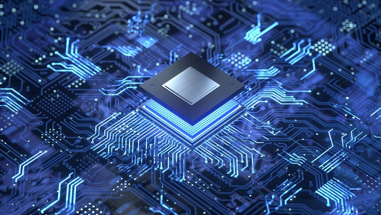
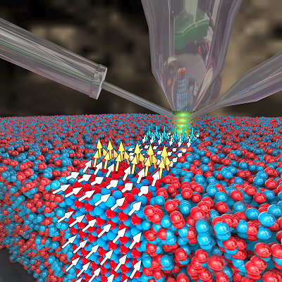
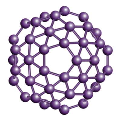
Modern electronic devices are unquestionably a symbol of our times, and chips, as their core component, act as brains, pushing boundaries and constantly developing the digital world. While they are often associated with computers, their use goes far beyond them, empowering numerous electronics devices. Microelectronics manufacturing relies on the unique properties of silicon, a semiconductor material that can act as both a conductor and an insulator. Semiconductor manufacturing process is complex, requiring specialized and highly precise equipment, controlled environmental conditions and cleanliness.
How is a semiconductor made?
It all starts with the wafer fabrication, which is then processed in multiple steps. The more advanced the chips are produced, the more steps are required. The first step is to extraction the raw silicon material from the sand, then turn it into a liquid and purify it, followed by the formation of a solid silicon crystal, which is called an ingot. It next needs to be cut into thin disks called wafers, polished, cleaned and the base for chip fabrication is ready. It is very important to maintain a spotless and smooth surface, as any fault can potentially affect the final product.
Deposition
The second stage in general provides the desired material properties. Deposition of thin layers of metals or oxides provides conductivity, insulation or semiconductivity, depending on the type of product. Purity in the semiconductor manufacturing process is more than critical, so further cleaning is required after this treatment too.
Photolithography
Now that the wafer has been prepared, the key phase – photolithography and etching – can begin.
It starts with the application of a very thin layer of photoresist, which is a material capable of reacting with light, to the wafer. This is followed by exposure to light through the photomask with a designed pattern, and the film is removed from the exposed areas, forming circuits on the surface.
The next process, gas- or liquid-based etching, is responsible for removing the thin layer of metals or oxides from step two, but only in the uncovered areas where the photoresist has been removed. The remaining material that was covered by the mask in the previous step ensures that the etchant will not affect the non-masked areas.
These two semiconductor production processes are repeated several times to achieve the desired complex architecture.
Ion Doping
Now that the earlier wafer fabrication steps have been carried out, the silicon substrate with the desired 3D architecture has many layers, and only the necessary areas are exposed, and impurity atoms are implanted in them. This changes the conductivity due to the specific structure of the silicon atoms, and after heat activation, micro-transistors are formed.
Metallization
In order to achieve the designed final layout and product properties, the transistors must be combined in a certain way. The metal alloys are deposited in sputtering machines, etched and the chip manufacturing process is almost complete.
After all these steps, the wafer fabrication process is finalized by quality control, cutting into individual chips and packaging. Now they can be combined with other electronic components and assembled into devices. XTPL S.A. has created an innovative dispensing technology that utilizes conductive nano-inks to form electrical connections. This method enables the printing of ultra-precise structures directly onto chips and other components, acting as printed wires to link inputs and outputs.
Semiconductor manufacturing processes are an amazing achievement of humanity, and their complexity is proof of how long the road has been traveled, but new challenges of miniaturization are still emerging. It’s remarkable how semiconductors have changed our lives and are undoubtedly shaping the future of the digital world, making it more innovative than ever!
Read the original article on Technology Org.

