He and his collaborators, representing multiple universities and national labs, detailed their innovative new technique studying how to better determine the nanoscale effects of radiation on materials in a recent paper in APL [Applied Physics Letters] Machine Learning.
UVA collaborates with Oak Ridge National Laboratory, which co-hosts Burns’ research.
The research features one of the largest labeled datasets of its kind and promises to advance the understanding of how materials behave not only under irradiated conditions, but potentially under other types of extremes as well.
Industries such as renewable energy, space exploration and advanced electronics stand to benefit from improved materials that can better withstand harsh environments.
For everyday consumers, the breakthrough could mean longer-lasting batteries, more reliable electronics and safer medical devices.
“Defects caused by radiation at the nanoscale can significantly affect performance and structural longevity,” said Burns, who became an assistant professor in August after joining the Department of Materials Science Engineering in 2022 as a Rising Scholar Research Scientist. “By examining the fundamental interactions within materials, we can devise better strategies to extend their lifetime.”
Tiny and Fast Changes
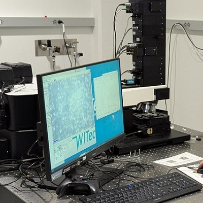
Transmission electron microscopy, or TEM, is an imaging technique that uses a beam of electrons to pass through very thin samples, often referred to as thin films because they’re so flat.
TEM can reveal atomic-level, nanoscale details about a specimen that are impossible to view with a light microscope. That might include crystal structures or small changes that occur due to surface interactions, making TEM an essential tool in materials science.
Scientists can also employ convolutional neural networks, or CNNs, to study changes over time. Unlike traditional models, CNNs learn from large groups of data all at once.
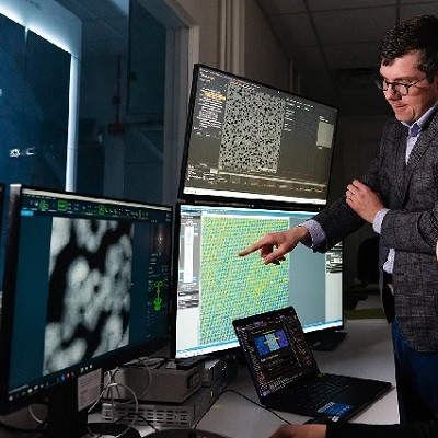
Burns’ team combined the two approaches, comparing its CNN results with traditional TEM images to assess the model's effectiveness at capturing nanoscale interactions.
“Our model reduces human error, accelerates analysis and quantifies rapid reactions,” Burns said. “However, accurate results depend on proper data preparation and fine-tuning model settings.”
Metals Differ in Their Defects
Using advanced time-series imaging techniques with the transmission electron microscope, the team compiled over 1,000 images capturing more than 250,000 defects formed during ion irradiation. These defects included helium bubbles and planar defects known as “dislocation loops.”
Key findings from the research highlight the complexities of defect classification. The study revealed that defects in materials such as copper and gold exhibit different behaviors compared to those in palladium. This distinction underscores the need for specialized analytical models to accurately study these materials under radiation.
One major challenge the researchers encountered was “drift,” where images can shift due to changes in the experimental environment, leading to potential inaccuracies. To address this, the team proposed the use of advanced techniques like denoising autoencoders, which help clean up images and improve data reliability.
Read the original article on University of Virginia.

