Take a photo with your phone and you might see wonderful details—leaves on a tree, strands of hair blowing in the wind. The width of that strand of hair is 100,000 nanometers wide. The best traditional laboratory microscope that uses light may capture details as small as 200 nanometers—the size of a large virus. The most advanced light microscope might discern features as small as 20-50 nanometers, or about the size of a large protein molecule.
Now engineers at Tufts have developed an imaging method that can see details down to 1.6 nanometers—the diameter of one DNA molecule.
The upper limit of existing imaging technology—called atomic force microscopy—has been used to detect single atoms, but the result is more akin to a rough black and white image. Atoms just appear as bumps on the surface. There is no “color” information about the type of atom or material.
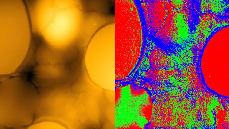
The new method, developed by a team led by Igor Sokolov, professor of mechanical engineering, and reported in Materials Today, uses atomic force microscopy, but combines it with physical measurements and machine learning to create a high resolution map of the material.
As the tiny atomic force microscope probe scans the surface of a sample, it can discern what type of molecule is underneath. For example, if the material is a composite of three different polymers, it can provide a color map of the distribution of molecule types and the nanoscale structure of the composite with a resolution of 1.6 nanometers.
The physical measurements include the contours of the surface, the energy lost in the microscope probe as it disconnects from the surface, and the length of the “neck” of material that stretches as the probe pulls away. Twelve different physical measurements in total are recorded simultaneously by using the advanced “ringing mode” of atomic force microscopy (also developed in Sokolov’s lab). This wealth of information is then processed through a machine learning algorithm that creates a profile for each type of material in the sample.
A Faster Way to Analyze New Materials
The new imaging technology has potential to be pivotal in studying materials that exhibit novel mechanical, electrical, or optical properties. Composite polymers can have superior strength-to-weight ratios, stiffness, flexibility, durability, heat resistance, and more. Car bumpers, for example, are made of a composite of polymers and particles of clay, whose development represented a breakthrough in increasing the durability, appearance, and safety of plastics used in automotive manufacturing.
Nanostructure imaging can help accelerate the development of new products. “Using this technique, we can get a much faster read on a polymer’s qualities,” said Sokolov. “For example, to understand how durable it is, we can expose the polymer to acid, heat, or UV light and then directly image what happens at near atomic resolution. Because the sensitivity and resolution of this technique is so high, we can see changes long before than any other technique, which might only detect changes at the micrometer scale.”
One application is improving the environmental sustainability of new plastics. By identifying novel plastic composites that degrade very smoothly, layer by layer, one could avoid the production of microplastics, which are typically produced by more uneven erosion of the polymers. As those plastics disintegrate, they contaminate the environment and end up in the food chain and ultimately, in human tissue.
Finding highly durable plastics that withstand a wide range of conditions could also lead to better, longer lasting materials, which would be highly desirable for applications like plumbing and building construction.
Health-care applications could include studies of tooth surfaces, to better understand how different substances and pathogens degrade teeth and to help develop coatings that may help protect them more effectively.
“Imaging at the nanoscale can help move polymer materials development toward a more analytical approach,” said Sokolov. “Plastics production today is an art based largely on trial and error. You mix polymers that you think might work well together, and you test under conditions that might replicate usage, aging, and environmental exposure, observing mostly macroscopic and microscopic changes in the material. By looking at the nanoscale changes, we can more quickly extrapolate to what might happen to these new materials over time.”
Read the original article on Tufts University.


