Their paper, published in ACS Applied Materials & Interfaces in late December 2024, could lead to more efficient and tunable photodetectors, paving the way for the next generation of light-sensing and multifunctional optoelectronic devices.
“Semiconductors are the key enabling technology for today’s electronics, from laptops to smartphones to AI applications,” said Xu Zhang, assistant professor of electrical and computer engineering. “They control the flow of electricity, acting as a bridge between conductors (which allow electricity to flow freely) and insulators (which block it).”
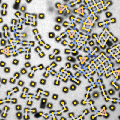
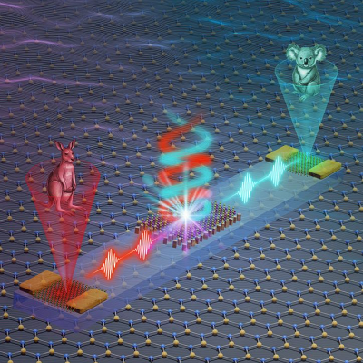
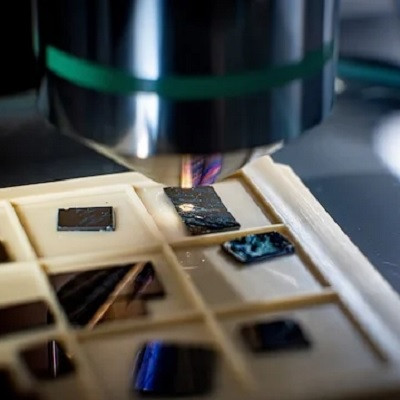
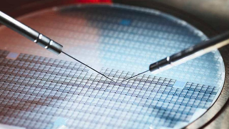
Zhang’s research group wanted to develop a certain kind of photodetector, a device capable of detecting light and which can be used in a variety of applications. To create this photodetector, the group needed to use materials that were an atom’s-width thick, or as close to 2d as is possible.
Today’s semiconductor industry relies heavily on CMOS (complementary metal-oxide-semiconductor) technology, which uses two types of semiconductor materials to enable energy-efficient electronic circuits, called p-type (or “positive-type”) and n-type (or “negative type”) materials.
“Making a good p-type semiconductor is not only important for this photodetector work, it is fundamentally important for almost all electronics” Zhang said.
While there are many kinds of 2d n-type materials available, 2d p-type materials are rarer—until now. CMU researchers seek a powerful new p-type semiconductor material, which could solve a critical bottleneck in the field of ultra-thin electronics.
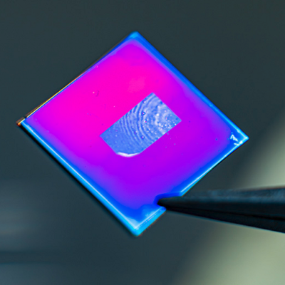
Luckily, they did know of a fitting material: tellurium. Tellurium is the 52nd element on the periodic table, located in group 16 a few periods (rows) below oxygen. It is a conductive metalloid, but most importantly, it acts like a p-type material. Even better, of the materials they tested, 2d tellurium had the highest mobility, or fastest conducting speed, at 1450 cm2/Vs, meaning that devices built with it can act extremely quickly. It also is much more stable in the air than the leading alternative, black phosphorus, so it does not easily degrade and stays fast and efficient for longer.
“This physical vapor deposition growth tellurium greatly enriches the 2d semiconductor material family,” said Tianyi Huang, graduate student in mechanical engineering and first author of the paper. “Its p-type property and outstanding electrical performance made it a strong candidate in various potential applications such as high-speed CMOS circuits, high-frequency RF [radio frequency] circuits, photodetectors, energy harvesting, and so on.”
Besides the ultra-light weight of the device, the tellurium-enabled photodetector is highly tunable, allowing its parameters to be changed so it can be used in a variety of applications, a property that is not true of other photodetectors. The researchers look forward to further developing this work to find its limits and best applications.
This interdisciplinary work was done through close collaboration with Sheng Shen, professor of mechanical engineering, and his group.
“With its unique properties, 2d p-type tellurium holds great promise for applications in photodetection and electronics. We are excited to further explore its potential in the near future,” Shen said.
As researchers continue to push the boundaries of 2d materials, this discovery marks a significant step toward a future where atom-thick electronics redefine speed, efficiency, and versatility.
Read the original article on Carnegie Mellon University.