Modern computing devices rely on memory technologies that are not only energy-hungry but physically separated from the processing units - leading to inefficiencies in speed and power. A promising alternative lies in spintronics, particularly racetrack memory (RTM), where data is stored in the form of movable magnetic domain walls (DWs) along nanowire-like “tracks.” These devices are non-volatile, energy-efficient, and can potentially unify memory and logic on a single chip.
To expand the design flexibility and integration potential of such devices, researchers have explored using freestanding membranes - thin films that are lifted off from their original substrates and transferred onto receiving surfaces, including patterned bases with 3D structures [1]. However, this process usually requires a buffer layer, such as magnesium oxide (MgO), to support high-quality magnetic layer growth. The buffer, while useful during fabrication, acts as an insulating barrier in the final device, preventing electrical or magnetic interaction with the underlying transfer bases.
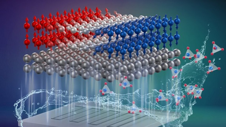
In a recently published paper in Adv. Mater. [2], scientists from the Max Planck Institute of Microstructure Physics have shown that this buffer layer is no longer necessary. In their new study, they demonstrate that a sacrificial oxide layer - Sr₃Al₂O₆ (SAO) - can directly support the growth of high-performance magnetic multilayers (Pt/Co/Ni/Co), enabling the fabrication of freestanding racetrack memory devices without any buffer layer. Remarkably, these buffer-free membranes exhibit better DW mobility than their buffered counterparts - despite being less than 4 nm thick.
A step further: the team transferred these membranes onto pre-patterned Pt underlayers, showing that the DW dynamics could be locally engineered - a key capability for future racetrack-based logic and memory architectures.
The study also confirms the remarkable robustness of these ultrathin racetracks. Devices maintain their performance after repeated mechanical bending, long-term ambient air exposure, thermal annealing, and electrical stress. The research not only deepens the understanding of interface engineering in freestanding magnetic films, but also opens a pathway to vertical or lateral coupling with functional substrates. This advances the vision of highly integrated, high-density spintronic devices.
Read the original article on Max Planck Institute of Microstructure Physics.