The ability to make a very miniature on/off switch changed the world. These tiny switches, known as transistors, make up the basis of all modern computing—they drive your cell phones, your bank transactions, your TV and much more.
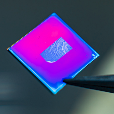
A team of scientists at the University of Chicago and Argonne National Laboratory have created an ultrathin transistor unlike any current design. Instead of larger 3-D layers of semiconductors, as in a traditional version, the new transistor is made from a layer of atomically thin semiconductor topped by a sheet of molecular crystal.
It runs on a fundamentally different principle than traditional transistors, using a phenomenon called charge localization, which had before only been achieved in materials that were cryogenically cooled to extremely low temperatures. The team’s new transistors, however, can run at room temperature.
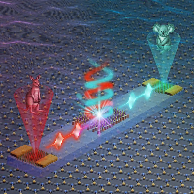
Their entire system is only four atoms thick, and the scientists measured its performance comparable to very good traditional transistors.
“This transistor behaves very differently from a conventional transistor, and it gives rise to a lot of interesting properties that conventional transistors do not have,” said Mengyu Gao, a postdoctoral fellow at UChicago and first author on the study, published Oct. 23 in Science.
The researchers hope the findings will open new avenues for technology, including in microelectronics and computing, but also power new fundamental discovery of the laws of nature.
Layered surprises
Since the 1950s, the transistors that power our modern lives have been made from silicon—hence the term Silicon Valley.
These systems have carried us very far, but as we seek to squeeze even more transistors into smaller spaces, engineers increasingly must turn three-dimensional devices into two-dimensional ones. Doing this with silicon has presented challenges, so scientists have been exploring alternatives.
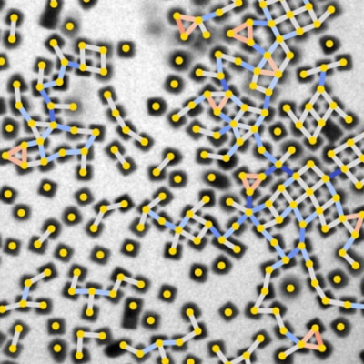
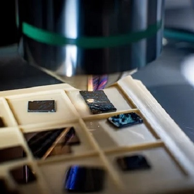
The laboratory of UChicago Prof. Jiwoong Park specializes in very thin-layered materials that can display unusual properties. In recent years, the Park lab has engineered new techniques to produce extremely pure and regular crystalline molecular films that are just a single atom thick.
In this case, they laid an atom-thick layer of molecules, called perylene diimide, on top of a three-atom-thick layer of semiconductor. When Gao tested the conductivity of this hybrid bilayer film, he found a strange phenomenon.
The material conducted electricity very well and continued to do so as he added more electrons—up until a certain tipping point. At that point, the material became an insulator, stopping the flow of current.
“Right away I saw this dip and knew that we had something interesting,” Gao said. “But when we tried digging down to explain what we saw, we started to realize this was something no one had seen before.”
When the scientists tested its performance as a transistor, they found it worked extremely well—nearly at the level of today’s high-performing silicon transistors.
Current trends
Conventional transistor theory could not explain this odd behavior. But after much painstaking work, the group developed a new model to describe what was happening.
Electrons normally move briskly through a semiconductor, carrying current that drives the transistor. In a typical transistor, the current is controlled by a voltage gate, which works like a gate in a water dam that controls the water level. Lowering the gate turns the transistor off, while higher gate voltage turns the transistor on. These “on” and “off” states, translated as 1 and 0, form the basis of binary computer language.
In the new material, electrons similarly move freely and carry more current when the gate is raised—until the voltage reaches a certain point. At that point, the electrons in the perylene molecular layer pair off with positive charges in the gate and settle down, interrupting the smooth flow of current. At this point, the transistor is turned off completely, even though it is still filled with electrons.
This is a phenomenon known as charge localization.
“What was striking was that once any electrons can go to the molecule layer, they all will,” said Park.
The finding is significant for several reasons.
Normal silicon transistors need to combine multiple different semiconductor layers that have been sprinkled with different types of atoms, known as n-type and p-type layers. But this new device doesn’t need that.
Further, the voltage needed overall is lower. Conserving power is always useful in an energy-hungry industry, and it could translate into less engineering needed for cooling, which is a top challenge in modern electronics, especially in the era of artificial intelligence.
The new transistor also shows an entirely novel behavior in a material that can be reliably made and integrated at large scales—scientists are always looking for different fundamental properties that could unlock new abilities in technology.
Lastly, but significantly, all of this can take place at room temperatures. This is helpful when designing practical applications, but the scientists see another plus.
“We have seen other systems that exhibit this charge localization phenomenon, but they all must be cooled down cryogenically to observe this effect,” said Gao.
The new system, therefore, is logistically a much easier way to study charge localization, which is a feature of interest in fundamental questions about physics.
The team is already exploring different configurations to tweak the material’s properties. For example, they hope to create what’s known as an electron crystal, which to date has only been achieved under very specialized conditions.
“What you see from this is that molecules can be used to design remarkable new electronic materials,” said Park. “We think this could really open new horizons.”
Read the original article on University of Chicago.