The group’s paper, “Magnetic Field Detection Limits for Ultraclean Graphene Hall Sensors,” published Aug. 20 in Nature Communications. The team was led by Katja Nowack, assistant professor of physics in the College of Arts and Sciences and the paper’s senior author.
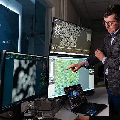
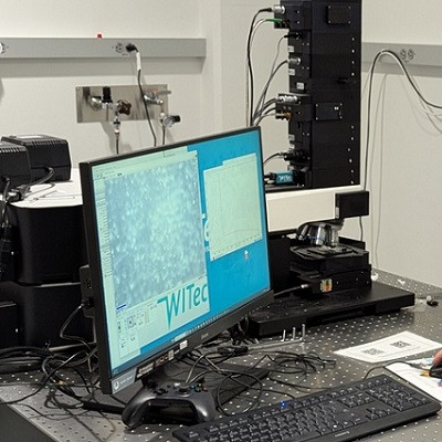
Nowack’s lab specializes in using scanning probes to conduct magnetic imaging. One of their go-to probes is the superconducting quantum interference device, or SQUID, which works well at low temperatures and in small magnetic fields.
“We wanted to expand the range of parameters that we can explore by using this other type of sensor, which is the Hall-effect sensor,” said doctoral student Brian Schaefer, the paper’s lead author. “It can work at any temperature, and we’ve shown it can work up to high magnetic fields as well. Hall sensors have been used at high magnetic fields before, but they’re usually not able to detect small magnetic field changes on top of that magnetic field.”
The Hall effect is a well-known phenomenon in condensed matter physics. When a current flows through a sample, it is bent by a magnetic field, creating a voltage across both sides of the sample that is proportional to the magnetic field.
Hall-effect sensors are used in a variety of technologies, from cellphones to robotics to anti-lock brakes. The devices are generally built out of conventional semiconductors like silicon and gallium arsenide. Nowack’s group decided to try a more novel approach.
The last decade has seen a boom in uses of graphene sheets – single layers of carbon atoms, arranged in a honeycomb lattice. But graphene devices often fall short of those made from other semiconductors when the graphene sheet is placed directly on a silicon substrate; the graphene sheet “crumples” on the nanoscale, inhibiting its electrical properties.
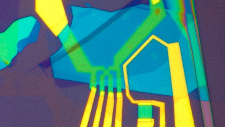
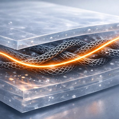
Nowack’s group adopted a recently developed technique to unlock graphene’s full potential – sandwiching it between sheets of hexagonal boron nitride. Hexagonal boron nitride has the same crystal structure as graphene but is an electrical insulator, which allows the graphene sheet to lie flat. Graphite layers in the sandwich structure act as electrostatic gates to tune the number of electrons that can conduct electricity in the graphene.
The sandwich technique was pioneered by co-author Lei Wang, a former postdoctoral researcher with the Kavli Institute at Cornell for Nanoscale Science. Wang also worked in the lab of co-senior author Paul McEuen, the John A. Newman Professor of Physical Science and co-chair of the Nanoscale Science and Microsystems Engineering (NEXT Nano) Task Force, part of the provost’s Radical Collaboration initiative.
“The encapsulation with hexagonal boron nitride and graphite makes the electronic system ultraclean,” Nowack said. “That allows us to work at even lower electron densities than we could before, and that’s favorable for boosting the Hall-effect signal we are interested in.”
The researchers were able to create a micron-scale Hall sensor that functions as well as the best Hall sensors reported at room temperature while outperforming any other Hall sensor at temperatures as low as 4.2 kelvins (or minus 452.11 degrees Fahrenheit).
The graphene sensors are so precise they can pick out tiny fluctuations in a magnetic field against a background field that is larger by six orders of magnitude (or a million times its size). Detecting such nuances is a challenge for even high-quality sensors because in a high magnetic field, the voltage response becomes nonlinear and therefore more difficult to parse.
Nowack plans to incorporate the graphene Hall sensor into a scanning probe microscope for imaging quantum materials and exploring physical phenomena, such as how magnetic fields destroy unconventional superconductivity and the ways that current flows in special classes of materials, such as topological metals.
“Magnetic field sensors and Hall sensors are important parts of many real-world applications,” Nowack said. “This work puts ultraclean graphene really on the map for being a superior material to build Hall probes out of. It wouldn’t be really practical for some applications because it’s hard to make these devices. But there are different pathways for materials growth and automated assembly of the sandwich that people are exploring. Once you have the graphene sandwich, you can put it anywhere and integrate it with existing technology.”
Read the original article on Cornell University.

