For several decades, scientists and engineers have been shrinking transistors to the point where their tiniest features are only comprised of tens of atoms. Ever since the first integrated circuits in the 1950s, the rate of progress in miniaturizing transistors has followed Moore's Law, which predicted the density of active components in integrated chips would double every two years.
As many of our readers know, progress in this direction has slowed down significantly in recent years. The main reason is that we are quickly approaching the physical limits of what's possible with existing materials and the most advanced manufacturing processes we have.

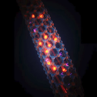
More specifically, we can't make transistor gates---which control the flow of current from the source to the drain---much smaller than 5 nm because of something called quantum tunneling that prevents them from working as intended. Materials like graphene and carbon nanotubes might be vital to making transistors even smaller thanks to their physical properties, but getting from there to building functional devices will take a while.
In a paper released this week, Chinese researchers explain they've created a transistor with the smallest gate length ever reported. This milestone was made possible by creatively utilizing graphene and molybdenum disulfide and stacking them into a staircase structure with two steps.
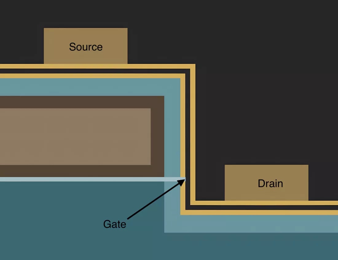
The structure of the side-wall transistor: The dark blue part is the silicon dioxide base, the brown is the aluminum covered in aluminum oxide, the thin, light blue strip is graphene, the yellow and black strip is molybdenum disulfide, and underneath it, you have the hafnium dioxide.
On the higher step, you have the source, and on top of the lower one, you have the drain. Both are made of a titanium palladium alloy separated by the surface of the stairs, which is made of a single sheet of a semiconductor material called molybdenum disulfide, itself resting on a layer of hafnium dioxide that acts as an electrical insulator.
The interior of the higher step is a literal sandwich of aluminum covered in aluminum oxide, which rests on top of a graphene sheet---a single layer of carbon atoms. The aluminum oxide acts as an electrical insulator, except for a small gap in the vertical wall of the higher step, where the graphene sheet is allowed to contact the molybdenum disulfide. The entire staircase structure rests on a thick layer of silicon dioxide.

The trick to this design is that the edge of the graphene sheet is used, which means that when the gate is set to the "on" state, it's only 0.34 nm wide---essentially the width of the graphene layer itself. Another notable feature of this "side-wall transistor" is its negligible current leakage due to higher off-state resistance. Manufacturers could leverage this quality for low-power applications. Best of all, it would be relatively easy to make, although many of the prototypes required quite a bit of voltage to drive.
Tsinghua University researcher Tian-Ling Ren co-authored the study and said this could be "the last node for Moore's law." He also believes going smaller than 0.34 nm for the gate size is almost impossible.
Of course, the researchers behind the new transistor only proved that a functional transistor could be made using one-atom thin materials without inventing a new process for precision positioning of the required layers. Reliably building billions of these side-wall transistors is still a distant dream but is a critical step in that direction, which fuels hope for faster, more power-efficient devices in the future.
In the meantime, Samsung, Intel, and TSMC are working hard on making gate-all-around (GAA-FET) transistors a reality and standardizing interconnects for chiplet designs.
Read the original article on TechSpot.