While X-rays probe the material’s crystal structure, a laser examines how it responds to light. When observed at crucial moments in the material’s creation, the combination of measurements can help scientists figure out how its structure and functionality are related.
The Impact
Researchers are interested in perovskite materials for their stellar ability to respond to and control light. These materials can absorb visible light more efficiently than silicon. They are also less effected by structural defects. This makes them promising for devices such as light-emitting diodes, detectors, and lasers. The knowledge obtained using the dual X-ray and laser spectroscopy technique could help improve the performance of perovskite materials. This combination of techniques could also allow manufacturers to automate real-time monitoring of materials synthesis for quality control.
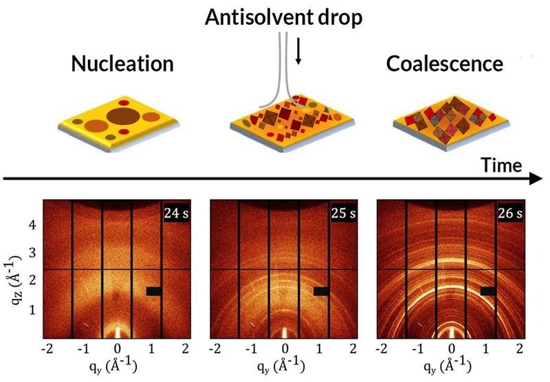
Schematic of the structures in a solar-cell precursor solution before, during, and after antisolvent is added to create the cell. X-ray scattering provides insights on the structural changes during the synthesis process.
Summary
Organic–inorganic halide perovskites consist of organic molecules (such as methylammonium) and inorganic metal halides (such as lead iodide). Despite their potential, perovskites have not yet been commercialized. This is due in part to the lack of reproducible synthesis of very high-quality perovskites and their long-term stability under operating conditions. To address these challenges, scientists used a custom-made analytical chamber at the Advanced Light Source, a Department of Energy Office of Science user facility. At the facility, the scientists used X-ray scattering to obtain structural information about perovskite evolution during synthesis, as well as laser-based spectroscopy to measure optical properties. The research team included scientists from the Technical University of Munich, Lawrence Berkeley National Laboratory, Polytechnique Fédérale de Lausanne, Switzerland, and Pennsylvania State University.
The simultaneous “split-screen” scattering and spectroscopy data provided complementary views of the crystallization kinetics, revealing how changes in optical response correlate with the evolution of the material’s structure. For example, during the synthesis process the addition of antisolvent correlates with a broad, intense photoluminescence peak and the rapid formation of polydisperse (nonuniform) nanocrystals. Subsequent structural reorganizations offered similar clues to the mechanisms underlying shifts in optical response. The researchers found the material’s structural evolution to proceed in four steps: nanocrystal nucleation upon the addition of antisolvent, cluster coalescence, thermal decomposition upon solvent evaporation, and the formation of cubic crystals in the thin film. Future studies of more complex perovskites will help optimize materials for advanced photovoltaic performance.
Read the original article on U.S. Department of Energy.