The next generation of 2D semiconductor materials doesn’t like what it sees when it looks in the mirror. Current synthesizing approaches to make single-layer nanosheets of semiconducting material for atomically thin electronics develop a peculiar “mirror twin” defect when the material is deposited on single-crystal substrates like sapphire. The synthesized nanosheet contains grain boundaries that act as a mirror, with the arrangement of atoms on each side organized in reflected opposition to one another.
This is a problem, according to researchers from the Penn State’s Two-Dimensional Crystal Consortium-Materials Innovation Platform (2DCC-MIP) and their collaborators. Electrons scatter when they hit the boundary, reducing the performance of devices like transistors. This is a bottleneck, the researchers said, for the advancement of next-generation electronics for applications such as Internet of Things and artificial intelligence. But now, the research team may have come up with a solution to correct this defect. They published their work in Nature Nanotechnology.
This study could have a significant impact on semiconductor research by enabling other researchers to reduce mirror twin defects, according to lead author Joan Redwing, director of 2DCC-MIP, especially as the field has increased attention and funding from the CHIPS and Science Act approved last year. The legislation’s authorization increased funding and other resources to boost America’s efforts to onshore the production and development of semiconductor technology.
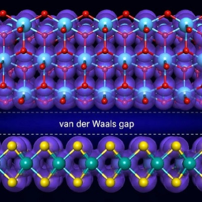
A single-layer sheet of tungsten diselenide — only three atoms thick — would make for a highly effective, atomically thin semiconductor to control and manipulate electrical current flow, according to Redwing. To make the nanosheet, the researchers use metal organic chemical vapor deposition (MOCVD), a semiconductor manufacturing technology that is used to deposit ultra-thin, single crystal layers onto a substrate, in this case a sapphire wafer.
While MOCVD is used in the synthesis of other materials, the 2DCC-MIP researchers pioneered its use for the synthesis of 2D semiconductors such as tungsten diselenide, Redwing said. Tungsten diselenide belongs to a class of materials called transition metal dichalcogenides that are three-atoms thick, with the tungsten metal sandwiched between non-metal selenide atoms, that manifests desirable semiconducting properties for advanced electronics.
“To achieve single-layer sheets with a high degree of crystalline perfection, we used sapphire wafers as a template to align the tungsten diselenide crystals as they deposit by MOCVD on the wafer surface,” said Redwing, who is also a distinguished professor of materials science and engineering and of electrical engineering at Penn State. “However, the tungsten diselenide crystals can align in opposite directions on the sapphire substrate. As the oppositely oriented crystals grow larger in size, they ultimately meet up with one another on the sapphire surface to form the mirror twin boundary.”
To solve this issue and get most of the tungsten diselenide crystals to align with the sapphire crystals, the researchers took advantage of “steps” on the sapphire surface. The sapphire single crystal that makes up the wafer is highly perfect in physics terms; however, it is not perfectly flat at the atomic level. There are steps on the surface that are a mere atom or two tall with flat areas between each step.
Here, Redwing said, the researchers found the suspected source of the mirror defect.
The step on the sapphire crystal surface is where the tungsten diselenide crystals tended to attach, but not always. The crystal alignment when attached to the steps tended to be in all one direction.
“If the crystals can all be aligned in the same direction, then mirror twin defects in the layer will be reduced or even eliminated,” Redwing said.
The researchers found that by controlling the MOCVD process conditions, most of the crystals could be made to attach to the sapphire at the steps. And during the experiments, they made a bonus discovery: If the crystals attach at the top of the step, they align in one crystallographic direction; if they attach at the bottom, they align in the opposite direction.
“We found that it was possible to get the majority of the crystals to attach at either the top or the bottom edge of the steps,” Redwing said, crediting experimental work performed by Haoyue Zhu, postdoctoral scholar, and Tanushree Choudhury, assistant research professor, in 2DCC-MIP. “This would provide a way to significantly reduce the number of mirror twin boundaries in the layers.”
Nadire Nayir, a postdoctoral scholar mentored by Distinguished University Professor Adri van Duin, led researchers in the 2DCC-MIP Theory/Simulation facility to develop a theoretical model of the atomic structure of sapphire surface to explain why the tungsten diselenide attached to the top or bottom edge of the steps. They theorized that if the surface of the sapphire was covered with selenium atoms, then they would attach to the bottom edge of the steps; if the sapphire is only partially covered so that the bottom edge of the step lacks selenium atom, then the crystals attached to the top.
To confirm this theory, the Penn State 2DCC-MIP researchers worked with Krystal York, a graduate student in the research group of Steven Durbin, professor of electrical and computer engineering at Western Michigan University. She contributed to the study as part of the 2DCC-MIP Resident Scholar Visitor Program. York learned how to grow tungsten diselenide thin films via MOCVD while using 2DCC-MIP facilities for her doctoral thesis research. Her experiments helped confirm that the method worked.
“While carrying out these experiments, Krystal observed that the direction of tungsten diselenide domains on sapphire switched when she varied the pressure in the MOCVD reactor,” Redwing said. “This experimental observation provided verification of the theoretical model that was developed to explain the attachment location of tungsten diselenide crystals on steps on the sapphire wafer.”
Wafer-scale tungsten diselenide samples on sapphire produced using this novel MOCVD process are available to researchers outside of Penn State via the 2DCC-MIP user program.
"Applications such as artificial intelligence and the Internet of Things will require further performance improvements as well as ways to reduce the energy consumption of electronics,” Redwing said. “High-quality 2D semiconductors based on tungsten diselenide and related materials are important materials that will play a role in next generation electronics.”
Read the original article on Pennsylvania State University.

