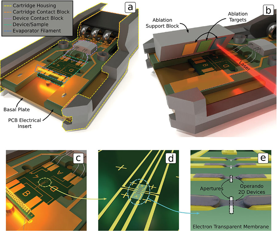
 Concept drawings illustrating simple approaches toward the development of the synthescope approach. a) An evaporator filament is incorporated on the end of a printed circuit board (PCB) that overhangs the device/sample. Electrical operation is facilitated through the use of existing electrical contacting holders. b) A strategy for laser ablation deposition is illustrated. This approach would require cutting an access notch in the holder cartridge and installation of a commercially available laser. Multiple ablation targets could be used to facilitate switching source materials. c) Magnified view of (a), showing electrical integration with a previously developed wafer-scale chip design. d) Electrical traces converge at the center of the chip where the operational devices are supported on an electron-transparent membrane (e) to be compatible with STEM imaging. (Reprinted with permission by Wiley-VCH Verlag) (click on image to enlarge)
With a synthescope, scientists could directly observe processes like nucleation, growth of crystals or nanoparticles, and incorporation of dopants into materials. By dynamically tuning parameters like temperature and deposition rate, they could optimize processes or switch material compositions on the fly. Such insights could prove invaluable for rational design of materials and devices.
For instance, the precise placement of just a few dopant atoms in key areas can greatly enhance the properties of 2D materials. And locating single atoms at the active sites of a catalyst can strongly influence its performance.
Realizing this vision will require further advances, from cleaner vacuum environments to redesigned hardware. But proof-of-principle experiments have already shown the feasibility of integrating localized material sources with STEMs. With focused research and development, synthescopes could open up a new paradigm for materials science within the next decade.
In their Perspective, the authors lay out a trajectory for progress in this emerging field. Early milestones like molecule-by-molecule deposition have already been achieved using STEMs' finely focused electron beams. But replicating traditional electron beam-induced deposition at the atomic scale presents challenges due to contamination issues. An alternate approach that uses beam damage to create reactive sites for atom incorporation shows more promise. Recent demonstrations of this technique achieved dopant patterning in 2D materials.
Ongoing improvements will require decoupling the atom supply from the imaging electron beam. The proposed synthescope could meet this need with integrated material sources. Controlled introduction of vaporized or laser-ablated atoms during beam patterning would enable precise atom-by-atom growth. Further developing strategies like feedback-controlled synthesis and multi-element deposition will maximize these tools' potential.
Guided by an unprecedented view into nanoscale synthesis, scientists will explore the vast possibilities for constructing matter from the atom up. With the synthetic power and analytical capabilities envisioned for synthescopes, researchers could uncover new nanoscale growth mechanisms and phenomena. These insights can then inform the design of more effective large-scale synthesis techniques.
In this way, synthescopes have the potential to revolutionize our fundamental understanding of materials formation while accelerating the development of atomically engineered structures for applications ranging from electronics to energy conversion and storage.
Concept drawings illustrating simple approaches toward the development of the synthescope approach. a) An evaporator filament is incorporated on the end of a printed circuit board (PCB) that overhangs the device/sample. Electrical operation is facilitated through the use of existing electrical contacting holders. b) A strategy for laser ablation deposition is illustrated. This approach would require cutting an access notch in the holder cartridge and installation of a commercially available laser. Multiple ablation targets could be used to facilitate switching source materials. c) Magnified view of (a), showing electrical integration with a previously developed wafer-scale chip design. d) Electrical traces converge at the center of the chip where the operational devices are supported on an electron-transparent membrane (e) to be compatible with STEM imaging. (Reprinted with permission by Wiley-VCH Verlag) (click on image to enlarge)
With a synthescope, scientists could directly observe processes like nucleation, growth of crystals or nanoparticles, and incorporation of dopants into materials. By dynamically tuning parameters like temperature and deposition rate, they could optimize processes or switch material compositions on the fly. Such insights could prove invaluable for rational design of materials and devices.
For instance, the precise placement of just a few dopant atoms in key areas can greatly enhance the properties of 2D materials. And locating single atoms at the active sites of a catalyst can strongly influence its performance.
Realizing this vision will require further advances, from cleaner vacuum environments to redesigned hardware. But proof-of-principle experiments have already shown the feasibility of integrating localized material sources with STEMs. With focused research and development, synthescopes could open up a new paradigm for materials science within the next decade.
In their Perspective, the authors lay out a trajectory for progress in this emerging field. Early milestones like molecule-by-molecule deposition have already been achieved using STEMs' finely focused electron beams. But replicating traditional electron beam-induced deposition at the atomic scale presents challenges due to contamination issues. An alternate approach that uses beam damage to create reactive sites for atom incorporation shows more promise. Recent demonstrations of this technique achieved dopant patterning in 2D materials.
Ongoing improvements will require decoupling the atom supply from the imaging electron beam. The proposed synthescope could meet this need with integrated material sources. Controlled introduction of vaporized or laser-ablated atoms during beam patterning would enable precise atom-by-atom growth. Further developing strategies like feedback-controlled synthesis and multi-element deposition will maximize these tools' potential.
Guided by an unprecedented view into nanoscale synthesis, scientists will explore the vast possibilities for constructing matter from the atom up. With the synthetic power and analytical capabilities envisioned for synthescopes, researchers could uncover new nanoscale growth mechanisms and phenomena. These insights can then inform the design of more effective large-scale synthesis techniques.
In this way, synthescopes have the potential to revolutionize our fundamental understanding of materials formation while accelerating the development of atomically engineered structures for applications ranging from electronics to energy conversion and storage.
 By
– Michael is author of three books by the Royal Society of Chemistry:
Nano-Society: Pushing the Boundaries of Technology,
Nanotechnology: The Future is Tiny, and
Nanoengineering: The Skills and Tools Making Technology Invisible
Copyright ©
Nanowerk LLC
By
– Michael is author of three books by the Royal Society of Chemistry:
Nano-Society: Pushing the Boundaries of Technology,
Nanotechnology: The Future is Tiny, and
Nanoengineering: The Skills and Tools Making Technology Invisible
Copyright ©
Nanowerk LLC
Nanowerk Newsletter
Get our Nanotechnology Spotlight updates to your inbox!
Become a Spotlight guest author! Join our large and growing group of guest contributors. Have you just published a scientific paper or have other exciting developments to share with the nanotechnology community? Here is how to publish on nanowerk.com.
