| Date | 9th, Sep 2018 |
|---|
Home > Press > Cannibalistic materials feed on themselves to grow new nanostructures
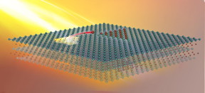 After a monolayer MXene is heated, functional groups are removed from both surfaces. Titanium and carbon atoms migrate from one area to both surfaces, creating a pore and forming new structures.
CREDIT
Oak Ridge National Laboratory, US Dept. of Energy; image by Xiahan Sang and Andy Sproles.
After a monolayer MXene is heated, functional groups are removed from both surfaces. Titanium and carbon atoms migrate from one area to both surfaces, creating a pore and forming new structures.
CREDIT
Oak Ridge National Laboratory, US Dept. of Energy; image by Xiahan Sang and Andy Sproles.
Abstract: Scientists at the Department of Energy's Oak Ridge National Laboratory induced a two-dimensional material to cannibalize itself for atomic "building blocks" from which stable structures formed.
Oak Ridge, TN | Posted on September 1st, 2018
The findings, reported in Nature Communications, provide insights that may improve design of 2D materials for fast-charging energy-storage and electronic devices.
"Under our experimental conditions, titanium and carbon atoms can spontaneously form an atomically thin layer of 2D transition-metal carbide, which was never observed before," said Xiahan Sang of ORNL.
He and ORNL's Raymond Unocic led a team that performed in situ experiments using state-of-the-art scanning transmission electron microscopy (STEM), combined with theory-based simulations, to reveal the mechanism's atomistic details.
"This study is about determining the atomic-level mechanisms and kinetics that are responsible for forming new structures of a 2D transition-metal carbide such that new synthesis methods can be realized for this class of materials," Unocic added.
The starting material was a 2D ceramic called a MXene (pronounced "max een"). Unlike most ceramics, MXenes are good electrical conductors because they are made from alternating atomic layers of carbon or nitrogen sandwiched within transition metals like titanium.
The research was a project of the Fluid Interface Reactions, Structures and Transport (FIRST) Center, a DOE Energy Frontier Research Center that explores fluid-solid interface reactions that have consequences for energy transport in everyday applications. Scientists conducted experiments to synthesize and characterize advanced materials and performed theory and simulation work to explain observed structural and functional properties of the materials. New knowledge from FIRST projects provides guideposts for future studies.
The high-quality material used in these experiments was synthesized by Drexel University scientists, in the form of five-ply single-crystal monolayer flakes of MXene. The flakes were taken from a parent crystal called "MAX," which contains a transition metal denoted by "M"; an element such as aluminum or silicon, denoted by "A"; and either a carbon or nitrogen atom, denoted by "X." The researchers used an acidic solution to etch out the monoatomic aluminum layers, exfoliate the material and delaminate it into individual monolayers of a titanium carbide MXene (Ti3C2).
The ORNL scientists suspended a large MXene flake on a heating chip with holes drilled in it so no support material, or substrate, interfered with the flake. Under vacuum, the suspended flake was exposed to heat and irradiated with an electron beam to clean the MXene surface and fully expose the layer of titanium atoms.
MXenes are typically inert because their surfaces are covered with protective functional groups--oxygen, hydrogen and fluorine atoms that remain after acid exfoliation. After protective groups are removed, the remaining material activates. Atomic-scale defects--"vacancies" created when titanium atoms are removed during etching--are exposed on the outer ply of the monolayer. "These atomic vacancies are good initiation sites," Sang said. "It's favorable for titanium and carbon atoms to move from defective sites to the surface." In an area with a defect, a pore may form when atoms migrate.
"Once those functional groups are gone, now you're left with a bare titanium layer (and underneath, alternating carbon, titanium, carbon, titanium) that's free to reconstruct and form new structures on top of existing structures," Sang said.
High-resolution STEM imaging proved that atoms moved from one part of the material to another to build structures. Because the material feeds on itself, the growth mechanism is cannibalistic.
"The growth mechanism is completely supported by density functional theory and reactive molecular dynamics simulations, thus opening up future possibilities to use these theory tools to determine the experimental parameters required for synthesizing specific defect structures," said Adri van Duin of Penn State.
Most of the time, only one additional layer [of carbon and titanium] grew on a surface. The material changed as atoms built new layers. Ti3C2 turned into Ti4C3, for example.
"These materials are efficient at ionic transport, which lends itself well to battery and supercapacitor applications," Unocic said. "How does ionic transport change when we add more layers to nanometer-thin MXene sheets?" This question may spur future studies.
"Because MXenes containing molybdenum, niobium, vanadium, tantalum, hafnium, chromium and other metals are available, there are opportunities to make a variety of new structures containing more than three or four metal atoms in cross-section (the current limit for MXenes produced from MAX phases)," Yury Gogotsi of Drexel University added. "Those materials may show different useful properties and create an array of 2D building blocks for advancing technology."
At ORNL's Center for Nanophase Materials Sciences (CNMS), Yu Xie, Weiwei Sun and Paul Kent performed first-principles theory calculations to explain why these materials grew layer by layer instead of forming alternate structures, such as squares. Xufan Li and Kai Xiao helped understand the growth mechanism, which minimizes surface energy to stabilize atomic configurations. Penn State scientists conducted large-scale dynamical reactive force field simulations showing how atoms rearranged on surfaces, confirming defect structures and their evolution as observed in experiments.
The researchers hope the new knowledge will help others grow advanced materials and generate useful nanoscale structures.
###
Research was supported as part of the FIRST Center, an Energy Frontier Research Center funded by the U.S. Department of Energy Office of Science. In situ aberration-corrected STEM imaging was conducted at CNMS, a U.S. Department of Energy Office of Science User Facility at ORNL. The research used resources of the National Energy Research Scientific Computing Center, a DOE Office of Science User Facility at Lawrence Berkeley National Laboratory.
####
About Oak Ridge National LaboratoryUT-Battelle manages ORNL for DOE's Office of Science. The single largest supporter of basic research in the physical sciences in the United States, the Office of Science is working to address some of the most pressing challenges of our time. For more information, please visit https://science.energy.gov/. --by Dawn Levy
For more information, please click here
Contacts:Dawn Levy
865-576-6448
Copyright © Oak Ridge National Laboratory
If you have a comment, please Contact us.
Issuers of news releases, not 7th Wave, Inc. or Nanotechnology Now, are solely responsible for the accuracy of the content.
Bookmark:


News and information
![]() Scientists unravel 'Hall effect' mystery in search for next generation memory storage devices August 19th, 2022
Scientists unravel 'Hall effect' mystery in search for next generation memory storage devices August 19th, 2022
![]() Researchers design new inks for 3D-printable wearable bioelectronics: Potential uses include printing electronic tattoos for medical tracking applications August 19th, 2022
Researchers design new inks for 3D-printable wearable bioelectronics: Potential uses include printing electronic tattoos for medical tracking applications August 19th, 2022
Laboratories
2 Dimensional Materials
![]() Buckyballs on gold are less exotic than graphene July 22nd, 2022
Buckyballs on gold are less exotic than graphene July 22nd, 2022
![]() Controlled synthesis of crystal flakes paves path for advanced future electronics June 17th, 2022
Controlled synthesis of crystal flakes paves path for advanced future electronics June 17th, 2022
![]() Solving the puzzle of 2D disorder: An interdisciplinary team developed a new method to characterize disorder in 2D materials June 17th, 2022
Solving the puzzle of 2D disorder: An interdisciplinary team developed a new method to characterize disorder in 2D materials June 17th, 2022
Govt.-Legislation/Regulation/Funding/Policy
![]() New chip ramps up AI computing efficiency August 19th, 2022
New chip ramps up AI computing efficiency August 19th, 2022
![]() Rice team eyes cells for sophisticated data storage: National Science Foundation backs effort to turn living cells into equivalent of computer RAM August 19th, 2022
Rice team eyes cells for sophisticated data storage: National Science Foundation backs effort to turn living cells into equivalent of computer RAM August 19th, 2022
![]() UNC Charlotte-led team invents new anticoagulant platform, offering hope for advances for heart surgery, dialysis, other procedures July 15th, 2022
UNC Charlotte-led team invents new anticoagulant platform, offering hope for advances for heart surgery, dialysis, other procedures July 15th, 2022
Possible Futures
![]() New chip ramps up AI computing efficiency August 19th, 2022
New chip ramps up AI computing efficiency August 19th, 2022
![]() Rice team eyes cells for sophisticated data storage: National Science Foundation backs effort to turn living cells into equivalent of computer RAM August 19th, 2022
Rice team eyes cells for sophisticated data storage: National Science Foundation backs effort to turn living cells into equivalent of computer RAM August 19th, 2022
Chip Technology
![]() New chip ramps up AI computing efficiency August 19th, 2022
New chip ramps up AI computing efficiency August 19th, 2022
![]() Scientists unravel 'Hall effect' mystery in search for next generation memory storage devices August 19th, 2022
Scientists unravel 'Hall effect' mystery in search for next generation memory storage devices August 19th, 2022
![]() Researchers design new inks for 3D-printable wearable bioelectronics: Potential uses include printing electronic tattoos for medical tracking applications August 19th, 2022
Researchers design new inks for 3D-printable wearable bioelectronics: Potential uses include printing electronic tattoos for medical tracking applications August 19th, 2022
Nanoelectronics
![]() Atomic level deposition to extend Moore's law and beyond July 15th, 2022
Atomic level deposition to extend Moore's law and beyond July 15th, 2022
![]() Controlled synthesis of crystal flakes paves path for advanced future electronics June 17th, 2022
Controlled synthesis of crystal flakes paves path for advanced future electronics June 17th, 2022
![]() Eyebrow-raising: Researchers reveal why nanowires stick to each other February 11th, 2022
Eyebrow-raising: Researchers reveal why nanowires stick to each other February 11th, 2022
Discoveries
![]() Scientists unravel 'Hall effect' mystery in search for next generation memory storage devices August 19th, 2022
Scientists unravel 'Hall effect' mystery in search for next generation memory storage devices August 19th, 2022
![]() Researchers design new inks for 3D-printable wearable bioelectronics: Potential uses include printing electronic tattoos for medical tracking applications August 19th, 2022
Researchers design new inks for 3D-printable wearable bioelectronics: Potential uses include printing electronic tattoos for medical tracking applications August 19th, 2022
![]() Visualizing nanoscale structures in real time: Open-source software enables researchers to see materials in 3D while they're still on the electron microscope August 19th, 2022
Visualizing nanoscale structures in real time: Open-source software enables researchers to see materials in 3D while they're still on the electron microscope August 19th, 2022
Materials/Metamaterials
![]() Strain-sensing smart skin ready to deploy: Nanotube-embedded coating detects threats from wear and tear in large structures July 15th, 2022
Strain-sensing smart skin ready to deploy: Nanotube-embedded coating detects threats from wear and tear in large structures July 15th, 2022
![]() New protocol for assessing the safety of nanomaterials July 1st, 2022
New protocol for assessing the safety of nanomaterials July 1st, 2022
![]() Nanotubes: a promising solution for advanced rubber cables with 60% less conductive filler June 1st, 2022
Nanotubes: a promising solution for advanced rubber cables with 60% less conductive filler June 1st, 2022
Announcements
![]() Scientists unravel 'Hall effect' mystery in search for next generation memory storage devices August 19th, 2022
Scientists unravel 'Hall effect' mystery in search for next generation memory storage devices August 19th, 2022
![]() Researchers design new inks for 3D-printable wearable bioelectronics: Potential uses include printing electronic tattoos for medical tracking applications August 19th, 2022
Researchers design new inks for 3D-printable wearable bioelectronics: Potential uses include printing electronic tattoos for medical tracking applications August 19th, 2022
![]() Visualizing nanoscale structures in real time: Open-source software enables researchers to see materials in 3D while they're still on the electron microscope August 19th, 2022
Visualizing nanoscale structures in real time: Open-source software enables researchers to see materials in 3D while they're still on the electron microscope August 19th, 2022
Interviews/Book Reviews/Essays/Reports/Podcasts/Journals/White papers/Posters
![]() Scientists unravel 'Hall effect' mystery in search for next generation memory storage devices August 19th, 2022
Scientists unravel 'Hall effect' mystery in search for next generation memory storage devices August 19th, 2022
![]() Researchers design new inks for 3D-printable wearable bioelectronics: Potential uses include printing electronic tattoos for medical tracking applications August 19th, 2022
Researchers design new inks for 3D-printable wearable bioelectronics: Potential uses include printing electronic tattoos for medical tracking applications August 19th, 2022
![]() Visualizing nanoscale structures in real time: Open-source software enables researchers to see materials in 3D while they're still on the electron microscope August 19th, 2022
Visualizing nanoscale structures in real time: Open-source software enables researchers to see materials in 3D while they're still on the electron microscope August 19th, 2022
Battery Technology/Capacitors/Generators/Piezoelectrics/Thermoelectrics/Energy storage
![]() Lithiophilic seeds and rigid arrays synergistic induced dendrite-free and stable Li anode towards long-life lithium-oxygen batteries July 22nd, 2022
Lithiophilic seeds and rigid arrays synergistic induced dendrite-free and stable Li anode towards long-life lithium-oxygen batteries July 22nd, 2022
![]() Crystal phase engineering offers glimpse of future potential, researchers say July 15th, 2022
Crystal phase engineering offers glimpse of future potential, researchers say July 15th, 2022
![]() Sieving carbons: Ideal anodes for high-energy sodium-ion batteries July 1st, 2022
Sieving carbons: Ideal anodes for high-energy sodium-ion batteries July 1st, 2022
![]() Two opposing approaches could give lithium-sulfur batteries a leg up over lithium-ion July 1st, 2022
Two opposing approaches could give lithium-sulfur batteries a leg up over lithium-ion July 1st, 2022
Research partnerships
![]() Crystal phase engineering offers glimpse of future potential, researchers say July 15th, 2022
Crystal phase engineering offers glimpse of future potential, researchers say July 15th, 2022
![]() New technology helps reveal inner workings of human genome June 24th, 2022
New technology helps reveal inner workings of human genome June 24th, 2022
![]() Boron nitride nanotube fibers get real: Rice lab creates first heat-tolerant, stable fibers from wet-spinning process June 24th, 2022
Boron nitride nanotube fibers get real: Rice lab creates first heat-tolerant, stable fibers from wet-spinning process June 24th, 2022
