Posted: Sep 28, 2018
(Nanowerk News) Nanostructures can increase the sensitivity of optical sensors enormously - provided that the geometry meets certain conditions and matches the wavelength of the incident light. This is because the electromagnetic field of light can be greatly amplified or reduced by the local nanostructure.
The HZB Young Investigator Group "Nano-SIPPE" headed by Prof. Christiane Becker is working to develop these kinds of nanostructures. Computer simulations are an important tool for this. Dr. Carlo Barth from the Nano-SIPPE team has now identified the most important patterns of field distribution in a nanostructure using machine learning, and has thereby explained the experimental findings very well for the first time (Communication Physics, "Machine learning classification for field distributions of photonic modes").
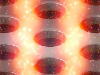 The computer simulation shows how the electromagnetic field is distributed in the silicon layer with hole pattern after excitation with a laser. Here, stripes with local field maxima are formed, so that quantum dots shine particularly strongly. (Image: Carlo Barth/HZB)
 examined in this paper consist of a silicon layer with a regular hole pattern coated with what are referred to as quantum dots made of lead sulphide. Excited with a laser, the quantum dots close to local field amplifications emit much more light than on an unordered surface.
This makes it possible to empirically demonstrate how the laser light interacts with the nanostructure.
examined in this paper consist of a silicon layer with a regular hole pattern coated with what are referred to as quantum dots made of lead sulphide. Excited with a laser, the quantum dots close to local field amplifications emit much more light than on an unordered surface.
This makes it possible to empirically demonstrate how the laser light interacts with the nanostructure.
The computer simulation shows how the electromagnetic field is distributed in the silicon layer with hole pattern after excitation with a laser. Here, stripes with local field maxima are formed, so that quantum dots shine particularly strongly. (Image: Carlo Barth/HZB)
