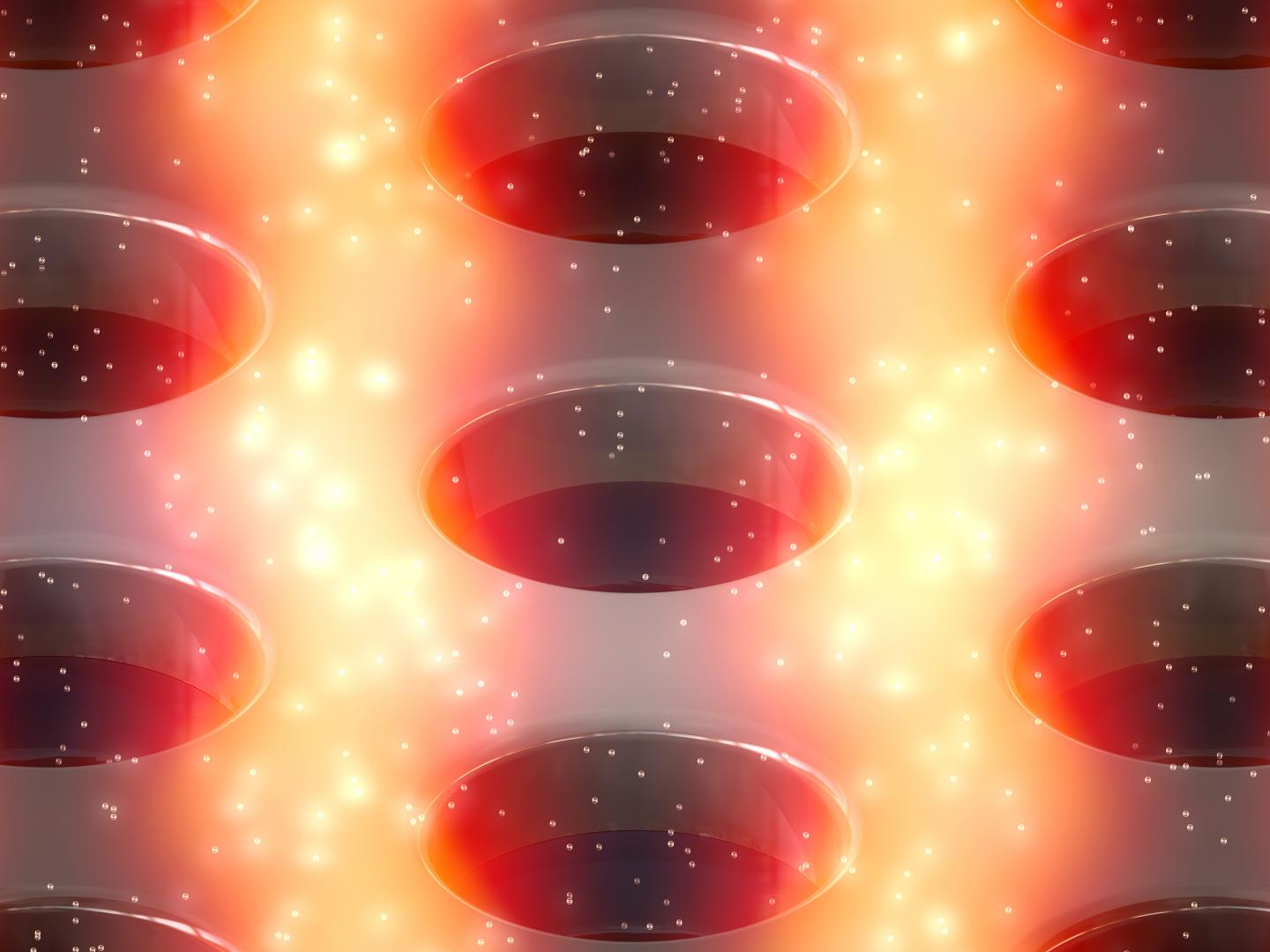
 The computer simulation shows how the electromagnetic field is distributed in the silicon layer with hole pattern after excitation with a laser. Here, stripes with local field maxima are formed, so that quantum dots shine particularly strongly. Courtesy of Carlo Barth/HZB.
To systematically record what happened when individual parameters of the nanostructure changed, the researchers calculated the 3D electric field distribution for each parameter set using software developed at the Zuse Institute Berlin. They analyzed this enormous amount of data using other computer programs, based on machine learning.
The computer simulation shows how the electromagnetic field is distributed in the silicon layer with hole pattern after excitation with a laser. Here, stripes with local field maxima are formed, so that quantum dots shine particularly strongly. Courtesy of Carlo Barth/HZB.
To systematically record what happened when individual parameters of the nanostructure changed, the researchers calculated the 3D electric field distribution for each parameter set using software developed at the Zuse Institute Berlin. They analyzed this enormous amount of data using other computer programs, based on machine learning.
“The computer has searched through the approximately 45,000 data records and grouped them into about 10 different patterns,” said researcher Carlo Barth. He worked with professor Christiane Becker to identify three basic patterns among these 10, in which the fields were amplified in various specific areas of the nanoholes.
This approach could allow photonic crystal membranes to be optimized for virtually any application, based on excitation amplification. For example, some biomolecules would accumulate preferentially along the hole edges, while others would accumulate along the plateaus between the holes, depending on the application.
Nanostructures can increase the sensitivity of optical sensors if their geometry meets certain conditions and matches the wavelength of the incident light. With the correct geometry and the right excitation by light, the maximum electric field amplification can be generated exactly at the attachment sites of the desired molecules, said the researchers. This could increase the sensitivity of optical sensors for cancer markers to the level of individual molecules, for example.
The research was published in Communication Physics (https://doi.org/10.1038/s42005-018-0060-1).
