Nov 01, 2018
(Nanowerk News) Graphene has held a great promise for applications since it was first isolated in 2004. But we still don’t use it in our large-scale technology, because we have no way of producing graphene on an industrial scale.
Leiden physicists have now visualized for the first time how atoms behave in between graphene and a substrate (Physical Review Materials, "Intrinsic stacking domains in graphene on silicon carbide: A pathway for intercalation"). This insight could be instrumental for future implementations of industrial graphene production.
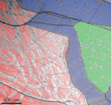 LEEM image of a graphene layer grown on a silicon carbide substrate. A red color indicates the presence of hydrogen atoms sandwiched between graphene and silicon carbide. The dark lines indicate strained regions in the graphene. The surrounding white areas show where the hydrogen atoms already left the interface. This shows that the lines act as tunnels where the hydrogen flows away faster. (Image: Leiden University)
In 2004, scientists managed to isolate a single layer of carbon atoms from a block of graphite. Since then, this so-called graphene layer has been praised for its high potential for all sorts of promising applications. It would enable high-speed transistors, economic electrical cars and delicate sensors.
So fast-forward to 2018, graphene is now the dominant building block of our computers, cars and gadgets, right? Wrong. There are still few large-scale graphene applications. The problem is that we haven’t figured out a way to produce graphene in high quality on the right substrate on an industrial scale.
LEEM image of a graphene layer grown on a silicon carbide substrate. A red color indicates the presence of hydrogen atoms sandwiched between graphene and silicon carbide. The dark lines indicate strained regions in the graphene. The surrounding white areas show where the hydrogen atoms already left the interface. This shows that the lines act as tunnels where the hydrogen flows away faster. (Image: Leiden University)
In 2004, scientists managed to isolate a single layer of carbon atoms from a block of graphite. Since then, this so-called graphene layer has been praised for its high potential for all sorts of promising applications. It would enable high-speed transistors, economic electrical cars and delicate sensors.
So fast-forward to 2018, graphene is now the dominant building block of our computers, cars and gadgets, right? Wrong. There are still few large-scale graphene applications. The problem is that we haven’t figured out a way to produce graphene in high quality on the right substrate on an industrial scale.
