| Date | 24th, May 2018 |
|---|
Home > Press > Columbia Researchers Squeeze Light into Nanoscale Devices and Circuits: Team is first to directly image propagation and dynamics of graphene plasmons at very low temperatures; findings could impact optical communications and signal processing
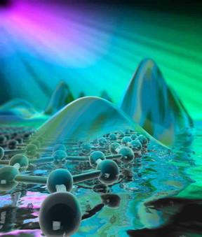 The best pictorial representation of a surface plasmon polariton is in terms of a �ripple� of electron density on the surface of graphene sample. Dmitri Basov/Columbia University
Abstract: As electronic devices and circuits shrink into the nanoscale, the ability to transfer data on a chip, at low power with little energy loss, is becoming a critical challenge. Over the past decade, squeezing light into tiny devices and circuits has been a major goal of nanophotonics researchers. Electronic oscillations at the surface of metals, known as surface plasmon polaritons or plasmons for short, have become an intense area of focus. Plasmons are hybrids of light (photons) and electrons in a metal. If researchers can harness this nanolight, they will be able to improve sensing, subwavelength waveguiding, and optical transmission of signals.
New York, NY | Posted on May 23rd, 2018
Columbia investigators have made a major breakthrough in this research, with their invention of a novel �home-built� cryogenic near-field optical microscope that has enabled them to directly image, for the first time, the propagation and dynamics of graphene plasmons at variable temperatures down to negative 250 degrees Celsius. The study was published online today in Nature.�Our temperature-dependent study now gives us direct physical insight into the fundamental physics of plasmon propagation in graphene,� says Dimitri N. Basov, professor of physics at Columbia University, who led the study together with colleagues Cory Dean (physics) and James Hone (mechanical engineering, Columbia Engineering). �This insight was impossible to attain in previous nanoimaging studies done at room temperature. We were particularly surprised at discovering, after many years of failed attempts to get anywhere close, that compact nanolight can travel along the surface of graphene for distances of many tens of microns without unwanted scattering. The physics limiting the travel range of nanolight is a fundamental finding of our study and may lead to new applications in sensors, imaging, and signal processing.� Basov, Dean, and Hone bring together years of experience in working with graphene, the one-atom-thick material that is one of the most promising candidates for novel photonic materials. Graphene�s optical properties are readily tunable and can be altered at ultrafast time scales. However, implementing nanolight without introducing unwanted dissipation in graphene has been very difficult to achieve. The Columbia researchers developed a practical approach to confining light to the nanoscale. They knew they could form plasmon-polaritons, or resonant modes, in the graphene that propagate through the material as hybrid excitations of light and mobile electrons. These plasmon-polariton modes can confine the energy of electromagnetic radiation, or light, down to the nanoscale. The challenge was how to visualize these waves with ultra-high spatial resolution, so that they could study the performance of plasmonic modes at varying temperatures. Alexander S. McLeod, a postdoctoral research scientist in the Basov Nano-optics Laboratory, built a unique microscope that enabled the team to explore the plasmon-polariton waves at high resolution while they cooled the graphene to cryogenic temperatures. Lowering the temperatures allowed them to �turn off� various scattering, or dissipation, mechanisms, one after another, as they cooled down their samples and learned which mechanisms were relevant. �Now that our novel nanoimaging capabilities are deployed to low temperatures, we can see directly the unmitigated wave propagation of collective light-and-charge excitations within graphene,� says McLeod, co-lead author of the study with Guangxin Ni, also a postdoctoral research scientist in Basov�s lab. �Often times in physics, as in life, seeing truly is believing! The record-breaking travel range of these waves shows they�re destined to take on a life of their own, funneling signals and information back and forth inside next-generation optical devices.� The study is the first to demonstrate the fundamental limitations for the propagation of plasmon polariton waves in graphene. The team found that graphene plasmons propagate ballistically, across tens of micrometers, throughout the tiny device. These plasmon modes are confined within a volume of space hundreds, if not thousands, of times smaller than that occupied by freely propagating light. Plasmons in graphene can be tuned and controlled via an external electric field, which gives graphene a big advantage over conventional plasmonic media such as metal surfaces, which are inherently non-tunable. Moreover, the lifetimes of plasmon waves in graphene are now found to exceed those in metals by a factor of 10 to a 100, while propagating over comparably longer distances. These features offer enormous advantages for graphene as a plasmonic medium in next-generation opto-electronic circuits. �Our results establish that graphene ranks among the best candidate materials for infrared plasmonics, with applications in imaging, sensing, and nano-scale manipulation of light,� says Hone. �Furthermore, our findings reveal the fundamental physics of processes that limit propagation of plasmon waves in graphene. This monumental insight will guide future efforts in nanostructure engineering, which may be able to remove the remaining roadblocks for long-range travel of versatile nanoconfined light within future optical devices.� The current study is the beginning of a series of low-temperature investigations focused on controlling and manipulating confined plasmons in nanoscale optoelectronic graphene devices. The team is now using low-temperature nanoimaging to explore novel plasmonics effects such as electrically-induced plasmonic reflection and modulation, topological chiral plasmons, and also superconducting plasmonics in the very recently discovered �magic angle� system of twisted bilayer graphene.
####
About Columbia University School of Engineering and Applied ScienceColumbia Engineering, based in New York City, is one of the top engineering schools in the U.S. and one of the oldest in the nation. Also known as The Fu Foundation School of Engineering and Applied Science, the School expands knowledge and advances technology through the pioneering research of its more than 200 faculty, while educating undergraduate and graduate students in a collaborative environment to become leaders informed by a firm foundation in engineering. The School�s faculty are at the center of the University�s cross-disciplinary research, contributing to the Data Science Institute, Earth Institute, Zuckerman Mind Brain Behavior Institute, Precision Medicine Initiative, and the Columbia Nano Initiative. Guided by its strategic vision, �Columbia Engineering for Humanity,� the School aims to translate ideas into innovations that foster a sustainable, healthy, secure, connected, and creative humanity.Columbia Engineering, based in New York City, is one of the top engineering schools in the U.S. and one of the oldest in the nation. Also known as The Fu Foundation School of Engineering and Applied Science, the School expands knowledge and advances technology through the pioneering research of its more than 200 faculty, while educating undergraduate and graduate students in a collaborative environment to become leaders informed by a firm foundation in engineering. The School�s faculty are at the center of the University�s cross-disciplinary research, contributing to the Data Science Institute, Earth Institute, Zuckerman Mind Brain Behavior Institute, Precision Medicine Initiative, and the Columbia Nano Initiative. Guided by its strategic vision, �Columbia Engineering for Humanity,� the School aims to translate ideas into innovations that foster a sustainable, healthy, secure, connected, and creative humanity.
For more information, please click here
Contacts:Holly EvartsDirector of Strategic Communications and Media Relations212-854-3206 (o)347-453-7408 (c)
Copyright © Columbia University School of Engineering and Applied Science
If you have a comment, please Contact us.
Issuers of news releases, not 7th Wave, Inc. or Nanotechnology Now, are solely responsible for the accuracy of the content.
Bookmark:


Imaging
![]() An artificial intelligence probe help see tumor malignancy July 1st, 2022
An artificial intelligence probe help see tumor malignancy July 1st, 2022
News and information
![]() Scientists unravel �Hall effect� mystery in search for next generation memory storage devices August 19th, 2022
Scientists unravel �Hall effect� mystery in search for next generation memory storage devices August 19th, 2022
![]() Researchers design new inks for 3D-printable wearable bioelectronics: Potential uses include printing electronic tattoos for medical tracking applications August 19th, 2022
Researchers design new inks for 3D-printable wearable bioelectronics: Potential uses include printing electronic tattoos for medical tracking applications August 19th, 2022
Graphene/ Graphite
![]() Buckyballs on gold are less exotic than graphene July 22nd, 2022
Buckyballs on gold are less exotic than graphene July 22nd, 2022
![]() A novel graphene based NiSe2 nanocrystalline array for efficient hydrogen evolution reaction July 15th, 2022
A novel graphene based NiSe2 nanocrystalline array for efficient hydrogen evolution reaction July 15th, 2022
![]() OCSiAl expands its graphene nanotube production capacities to Europe June 17th, 2022
OCSiAl expands its graphene nanotube production capacities to Europe June 17th, 2022
Plasmonics
![]() A new dimension in magnetism and superconductivity launched November 5th, 2021
A new dimension in magnetism and superconductivity launched November 5th, 2021
![]() Patterning silicon at the one nanometer scale: Scientists engineer materials� electrical and optical properties with plasmon engineering August 13th, 2021
Patterning silicon at the one nanometer scale: Scientists engineer materials� electrical and optical properties with plasmon engineering August 13th, 2021
![]() TPU scientists offer new plasmon energy-based method to remove CO2 from atmosphere March 19th, 2021
TPU scientists offer new plasmon energy-based method to remove CO2 from atmosphere March 19th, 2021
Govt.-Legislation/Regulation/Funding/Policy
![]() New chip ramps up AI computing efficiency August 19th, 2022
New chip ramps up AI computing efficiency August 19th, 2022
![]() Rice team eyes cells for sophisticated data storage: National Science Foundation backs effort to turn living cells into equivalent of computer RAM August 19th, 2022
Rice team eyes cells for sophisticated data storage: National Science Foundation backs effort to turn living cells into equivalent of computer RAM August 19th, 2022
![]() UNC Charlotte-led team invents new anticoagulant platform, offering hope for advances for heart surgery, dialysis, other procedures July 15th, 2022
UNC Charlotte-led team invents new anticoagulant platform, offering hope for advances for heart surgery, dialysis, other procedures July 15th, 2022
Possible Futures
![]() New chip ramps up AI computing efficiency August 19th, 2022
New chip ramps up AI computing efficiency August 19th, 2022
![]() Rice team eyes cells for sophisticated data storage: National Science Foundation backs effort to turn living cells into equivalent of computer RAM August 19th, 2022
Rice team eyes cells for sophisticated data storage: National Science Foundation backs effort to turn living cells into equivalent of computer RAM August 19th, 2022
Chip Technology
![]() New chip ramps up AI computing efficiency August 19th, 2022
New chip ramps up AI computing efficiency August 19th, 2022
![]() Scientists unravel �Hall effect� mystery in search for next generation memory storage devices August 19th, 2022
Scientists unravel �Hall effect� mystery in search for next generation memory storage devices August 19th, 2022
![]() Researchers design new inks for 3D-printable wearable bioelectronics: Potential uses include printing electronic tattoos for medical tracking applications August 19th, 2022
Researchers design new inks for 3D-printable wearable bioelectronics: Potential uses include printing electronic tattoos for medical tracking applications August 19th, 2022
Optical computing/Photonic computing
![]() Deep-ultraviolet nonlinear optical crystals: Concept development and materials discovery July 8th, 2022
Deep-ultraviolet nonlinear optical crystals: Concept development and materials discovery July 8th, 2022
![]() Photoinduced large polaron transport and dynamics in organic-inorganic hybrid lead halide perovskite with terahertz probes July 8th, 2022
Photoinduced large polaron transport and dynamics in organic-inorganic hybrid lead halide perovskite with terahertz probes July 8th, 2022
Nanoelectronics
![]() Atomic level deposition to extend Moore�s law and beyond July 15th, 2022
Atomic level deposition to extend Moore�s law and beyond July 15th, 2022
![]() Controlled synthesis of crystal flakes paves path for advanced future electronics June 17th, 2022
Controlled synthesis of crystal flakes paves path for advanced future electronics June 17th, 2022
![]() Eyebrow-raising: Researchers reveal why nanowires stick to each other February 11th, 2022
Eyebrow-raising: Researchers reveal why nanowires stick to each other February 11th, 2022
Discoveries
![]() Scientists unravel �Hall effect� mystery in search for next generation memory storage devices August 19th, 2022
Scientists unravel �Hall effect� mystery in search for next generation memory storage devices August 19th, 2022
![]() Researchers design new inks for 3D-printable wearable bioelectronics: Potential uses include printing electronic tattoos for medical tracking applications August 19th, 2022
Researchers design new inks for 3D-printable wearable bioelectronics: Potential uses include printing electronic tattoos for medical tracking applications August 19th, 2022
![]() Visualizing nanoscale structures in real time: Open-source software enables researchers to see materials in 3D while they're still on the electron microscope August 19th, 2022
Visualizing nanoscale structures in real time: Open-source software enables researchers to see materials in 3D while they're still on the electron microscope August 19th, 2022
Announcements
![]() Scientists unravel �Hall effect� mystery in search for next generation memory storage devices August 19th, 2022
Scientists unravel �Hall effect� mystery in search for next generation memory storage devices August 19th, 2022
![]() Researchers design new inks for 3D-printable wearable bioelectronics: Potential uses include printing electronic tattoos for medical tracking applications August 19th, 2022
Researchers design new inks for 3D-printable wearable bioelectronics: Potential uses include printing electronic tattoos for medical tracking applications August 19th, 2022
![]() Visualizing nanoscale structures in real time: Open-source software enables researchers to see materials in 3D while they're still on the electron microscope August 19th, 2022
Visualizing nanoscale structures in real time: Open-source software enables researchers to see materials in 3D while they're still on the electron microscope August 19th, 2022
Interviews/Book Reviews/Essays/Reports/Podcasts/Journals/White papers/Posters
![]() Scientists unravel �Hall effect� mystery in search for next generation memory storage devices August 19th, 2022
Scientists unravel �Hall effect� mystery in search for next generation memory storage devices August 19th, 2022
![]() Researchers design new inks for 3D-printable wearable bioelectronics: Potential uses include printing electronic tattoos for medical tracking applications August 19th, 2022
Researchers design new inks for 3D-printable wearable bioelectronics: Potential uses include printing electronic tattoos for medical tracking applications August 19th, 2022
![]() Visualizing nanoscale structures in real time: Open-source software enables researchers to see materials in 3D while they're still on the electron microscope August 19th, 2022
Visualizing nanoscale structures in real time: Open-source software enables researchers to see materials in 3D while they're still on the electron microscope August 19th, 2022
Tools
![]() Atomic level deposition to extend Moore�s law and beyond July 15th, 2022
Atomic level deposition to extend Moore�s law and beyond July 15th, 2022
![]() New technology helps reveal inner workings of human genome June 24th, 2022
New technology helps reveal inner workings of human genome June 24th, 2022
![]() Snapshot measurement of single nanostructure�s circular dichroism March 25th, 2022
Snapshot measurement of single nanostructure�s circular dichroism March 25th, 2022
Military
![]() New chip ramps up AI computing efficiency August 19th, 2022
New chip ramps up AI computing efficiency August 19th, 2022
![]() Strain-sensing smart skin ready to deploy: Nanotube-embedded coating detects threats from wear and tear in large structures July 15th, 2022
Strain-sensing smart skin ready to deploy: Nanotube-embedded coating detects threats from wear and tear in large structures July 15th, 2022
![]() Boron nitride nanotube fibers get real: Rice lab creates first heat-tolerant, stable fibers from wet-spinning process June 24th, 2022
Boron nitride nanotube fibers get real: Rice lab creates first heat-tolerant, stable fibers from wet-spinning process June 24th, 2022
Grants/Sponsored Research/Awards/Scholarships/Gifts/Contests/Honors/Records
![]() New chip ramps up AI computing efficiency August 19th, 2022
New chip ramps up AI computing efficiency August 19th, 2022
![]() UNC Charlotte-led team invents new anticoagulant platform, offering hope for advances for heart surgery, dialysis, other procedures July 15th, 2022
UNC Charlotte-led team invents new anticoagulant platform, offering hope for advances for heart surgery, dialysis, other procedures July 15th, 2022
![]() Photoinduced large polaron transport and dynamics in organic-inorganic hybrid lead halide perovskite with terahertz probes July 8th, 2022
Photoinduced large polaron transport and dynamics in organic-inorganic hybrid lead halide perovskite with terahertz probes July 8th, 2022
![]() Luisier wins SNSF Advanced Grant to develop simulation tools for nanoscale devices July 8th, 2022
Luisier wins SNSF Advanced Grant to develop simulation tools for nanoscale devices July 8th, 2022
Photonics/Optics/Lasers
![]() �Life-like� lasers can self-organise, adapt their structure, and cooperate July 15th, 2022
�Life-like� lasers can self-organise, adapt their structure, and cooperate July 15th, 2022
![]() Electrically driven single microwire-based single-mode microlaser July 8th, 2022
Electrically driven single microwire-based single-mode microlaser July 8th, 2022
![]() Deep-ultraviolet nonlinear optical crystals: Concept development and materials discovery July 8th, 2022
Deep-ultraviolet nonlinear optical crystals: Concept development and materials discovery July 8th, 2022
