Jan 09, 2019
(Nanowerk Spotlight) Liquid crystals (LCs) are optically anisotropic materials, and they are widely used in electro-optical display technology, known as liquid crystal displays (LCDs). Understanding the alignment phenomena of a nematic LC on a surface remains an important area of research, as the alignment process determines the LC’s molecular orientation and conformation – which influence the LC’s optical and electro-optical characteristics in LCDs.
The planar-alignment layers are utilized to create an easy axis of the nematic director of the LC in the LCD. The conventional planar-alignment layer is a rubbed polyimide (PI)-coated surface. On the unidirectionally rubbed PI alignment substrate, the LC molecules align with alkyl side chains along the rubbing direction, creating a uniform planar director profile on the substrate.
However, the conventional rubbed PI alignment process has some disadvantages. The occurrence of fiber dust during the rubbing process of the PI contaminates the LC. Uneven rubbing creates a wide distribution of pre-tilt angles of the LC—which causes a non-uniform brightness in the LCD panel.
The PI alignment layers can inject free ion impurities into the LC. Therefore, studying various LC-substrate interactions, and then, developing alternate LC alignment methods (e.g., oblique SiO evaporation, microgroove grating surface fabrication, photoalignment technology, etc.) is an important research direction for optical display applications.
Associate Professor Rajratan Basu and his student Midshipman Lukas Atwood in the Department of Physics at the United States Naval Academy report an interesting phenomenon of two-dimensional (2D) hexagonal boron nitride (h-BN)-induced planar-alignment of a nematic LC and the subsequent optical and electro-optical effects.
They report their findings in the January 7 issue of Optics Express ("Two-dimensional hexagonal boron nitride nanosheet as the planar-alignment agent in a liquid crystal-based electro-optic device"). This work was supported by the Office of Naval Research.
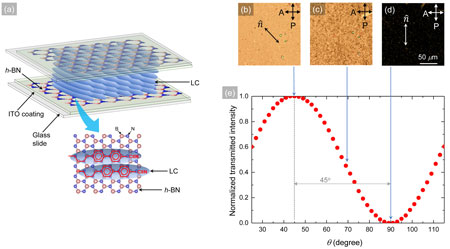
 Figure 1: (a) A schematic representation of the h-BN-based liquid crystal cell containing a layer of ITO and an h-BN film on each glass slide. Below the cell, the alignment of nematic LC molecules (ellipsoids) on 2D h-BN (honeycomb structure) is illustrated. The epitaxial interaction between the LC and the h-BN lattice is schematically shown by matching the LC’s benzene rings on the h-BN-honeycomb structure. (b), (c), and (d) Micrographs of the bright, intermediate, and dark states, respectively, under the crossed polarized optical microscope of the h-BN-based LC cell filled with LC E7. (e) Normalized transmitted intensity as a function of θ, the angle between the average LC director in the cell and the analyzer. The white bar in micrograph-(f) presents 50 µm. (Image: United States Naval Academy) (click on image to enlarge)
“The sp2 conjugated 2D boron nitride nanosheet forms a honeycomb structure of alternating boron and nitrogen atoms with a lattice spacing of 1.44 Å. This 2D h-BN is an insulator, which has a very high structural, thermal, and chemical stability,” Basu explains. “In the LC, the C-C bond length in the hexagonal benzene rings is 1.40 Å. Therefore, the hexagon of the benzene ring and the hexagon in the h-BN lattice have almost the same size. This nano-architectural symmetry between the hexagons in both the species causes the benzene rings of the LC coherently align on the hexagonal lattice of h-BN. This spontaneous epitaxial alignment mechanism of the LC on the hexagonal lattice is the fundamental principle in our experiment for using the 2D h-BN as the planar-alignment agent in this electro-optic LC device.”
“This h-BN-based LC cell shows the typical electro-optical effect when an electric field is applied via ITO electrodes,” Basu continues. “The dielectric measurement across this h-BN-based electro-optic cell shows a standard Fréedericksz transition of the LC, confirming that the 2D h-BN, as the planar-alignment agent, supplies adequate anchoring energy – which can be overcome by the Fréedericksz threshold voltage.”
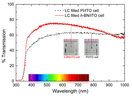
Finally, Basu and Atwood show that the h-BN-based LC cell exhibits more optical transparency than the commercial PI-based LC cell.
 Figure 2: Optical transmission as a function wavelength for the LC-filled PI/ITO cell and the LC-filled h-BN/ITO listed in the legend. The visible wavelength range is shown in the x-axis. The inset pictures show the two cells. (Image: United States Naval Academy) (click on image to enlarge)
Basu and Atwood note that in the commercial LC cell, the total thickness of the two rubbed planar-aligning PI layers is about 120 nm. On the other hand, the thickness of a 2D h-BN film is around 0.3 nm. Replacing both the PI alignment layers with the 2D h-BN on both sides decreases this effective thickness to less than 1 nm – which leads to the potential to increase the optical transmission over a broad spectral range in this LC-based electro-optic device.
Provided by the United States Naval Academy as a Nanowerk exclusive
 Figure 1: (a) A schematic representation of the h-BN-based liquid crystal cell containing a layer of ITO and an h-BN film on each glass slide. Below the cell, the alignment of nematic LC molecules (ellipsoids) on 2D h-BN (honeycomb structure) is illustrated. The epitaxial interaction between the LC and the h-BN lattice is schematically shown by matching the LC’s benzene rings on the h-BN-honeycomb structure. (b), (c), and (d) Micrographs of the bright, intermediate, and dark states, respectively, under the crossed polarized optical microscope of the h-BN-based LC cell filled with LC E7. (e) Normalized transmitted intensity as a function of θ, the angle between the average LC director in the cell and the analyzer. The white bar in micrograph-(f) presents 50 µm. (Image: United States Naval Academy) (click on image to enlarge)
“The sp2 conjugated 2D boron nitride nanosheet forms a honeycomb structure of alternating boron and nitrogen atoms with a lattice spacing of 1.44 Å. This 2D h-BN is an insulator, which has a very high structural, thermal, and chemical stability,” Basu explains. “In the LC, the C-C bond length in the hexagonal benzene rings is 1.40 Å. Therefore, the hexagon of the benzene ring and the hexagon in the h-BN lattice have almost the same size. This nano-architectural symmetry between the hexagons in both the species causes the benzene rings of the LC coherently align on the hexagonal lattice of h-BN. This spontaneous epitaxial alignment mechanism of the LC on the hexagonal lattice is the fundamental principle in our experiment for using the 2D h-BN as the planar-alignment agent in this electro-optic LC device.”
“This h-BN-based LC cell shows the typical electro-optical effect when an electric field is applied via ITO electrodes,” Basu continues. “The dielectric measurement across this h-BN-based electro-optic cell shows a standard Fréedericksz transition of the LC, confirming that the 2D h-BN, as the planar-alignment agent, supplies adequate anchoring energy – which can be overcome by the Fréedericksz threshold voltage.”
Finally, Basu and Atwood show that the h-BN-based LC cell exhibits more optical transparency than the commercial PI-based LC cell.
 Figure 2: Optical transmission as a function wavelength for the LC-filled PI/ITO cell and the LC-filled h-BN/ITO listed in the legend. The visible wavelength range is shown in the x-axis. The inset pictures show the two cells. (Image: United States Naval Academy) (click on image to enlarge)
Basu and Atwood note that in the commercial LC cell, the total thickness of the two rubbed planar-aligning PI layers is about 120 nm. On the other hand, the thickness of a 2D h-BN film is around 0.3 nm. Replacing both the PI alignment layers with the 2D h-BN on both sides decreases this effective thickness to less than 1 nm – which leads to the potential to increase the optical transmission over a broad spectral range in this LC-based electro-optic device.
Provided by the United States Naval Academy as a Nanowerk exclusive
Nanowerk Newsletter
Get our Nanotechnology Spotlight updates to your inbox!
Become a Spotlight guest author! Join our large and growing group of guest contributors. Have you just published a scientific paper or have other exciting developments to share with the nanotechnology community? Here is how to publish on nanowerk.com.

