| Date | 29th, May 2018 |
|---|
Home > Press > Novel method to fabricate nanoribbons from speeding nano droplets
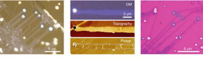 From left are 1) Optical images of MoS2 ribbons grown on a NaCl crystal, 2) Optical microscopy (OM) and corresponding AFM topography and phase images of a ribbon, and 3) Optical image of the ribbons transferred onto a SiO2/Si substrate.
CREDIT
UNIST
From left are 1) Optical images of MoS2 ribbons grown on a NaCl crystal, 2) Optical microscopy (OM) and corresponding AFM topography and phase images of a ribbon, and 3) Optical image of the ribbons transferred onto a SiO2/Si substrate.
CREDIT
UNIST
Abstract: An international team of researchers, affiliated with UNIST has discovered a novel method for the synthesis of ultrathin semiconductors. This is a unique growth mechanism, which yielded nanoscopic semiconductor ribbons that are only a few atoms thick.
Ulsan, Korea | Posted on May 29th, 2018
This breakthrough has been jointly conducted by Distinguished Professor Feng Ding and Dr. Wen Zhao from the Center for Multidimensional Carbon Materials (CMCM), within the Institute for Basic Science (IBS) at UNIST, in collaboration with the National University of Singapore (NUS), the National Institute for Materials Science (NIMS), the National Institute of Advanced Industrial Science and Technology (AIST), and Shenzhen University.
In the study, the research team has successfully fabricated MoS2 nanoribbons via vapour-liquid-solid (VLS) growth mechanism, a type of chemical vapour deposition (CVD) process.
"Synthesis of vertically elongated structure via VLS growth mechanism."
Chemical vapor deposition or CVD is a generic name for a group of processes whereby a solid material is deposited from a vapor by a chemical reaction occurring on or in the vicinity of a normally heated substrate surface. It is the most widely adopted industrial techniques for producing semiconducting thin films and nanostructures.
"The range of structures that can be controllably synthesized by the current methods is still limited in terms of morphology, spatial selectivity, crystal orientation, layer number and chemical composition," the research team noted. "Therefore, developing versatile growth methods is essential to the realization of highly integrated electronic and photonic devices based on these materials.
"The current CVD-based growth process relies on the inherent dynamics of the precursors to diffuse and self-organize on the substrate surface, which results in crystallites with characteristic triangular or hexagonal shapes," says Dr. Zhao. "This unique growth mechanism of the nanoscopic semiconductor ribbons that are only a few atoms thick is an exciting discovery." In the study, she performed density functional theory based molecular dynamic (DFT-MD) simulations of the MoS2 precipitation process.
The proposed mechanism of VLS growth differs from commonly known CVD technique, as it involves the precursors introduced in the vapour phase form a liquid droplet intermediate before condensing into a solid product.
The team noted that the morphology of the growth product was, however, unlike what is normally expected from a VLS growth, which typically yields cylindrical or tubular structures rather than ribbons. Their observation suggests that the liquid droplet migrates on the substrate surface in a rather ordered manner, leaving behind a track of ultrathin crystal.
"Because the liquid droplet migrates on the substrate surface in a rather ordered manner, the morphology of the growth product yielded cylindrical or tubular structures rather than ribbons." says Dr. Zhao.
This time, however, the horizontal growth of predominantly monolayer MoS2 ribbons was obtained via VLS growth, a unique growth mechanism that has not been reported until now.
Their observation revealed that the VLS growth of monolayer MoS2 is triggered by the reaction between MoO3 and NaCl, which results in the formation of molten Na-Mo-O droplets. These droplets mediate the growth of MoS2 ribbons in the 'crawling mode' when saturated with sulfur. The locally well-defined orientations of the ribbons reveal the regular horizontal motion of the droplets during growth.
"Assisting the growth of MoS2 ribbons, like painting with a an ink droplet."
In order to gain insight into the liquid-solid transformation, Professor Ding's team performed density functional theory based molecular dynamic (DFT-MD) sumulations of the precipitation process. The simulation showed the attachment of molybdenum (Mo) and sulfur (S) to the previously established MoS2.
"It is worth noting that MoS2 is not oxidized despite the presence of large numbers of oxygen atoms," says the research team. "We also observe the nucleation of MoS2 clusters in regions that are rich in Mo and S atoms, further supporting the feasibility of liquid-mediated nucleation and growth of MoS2."
"This study has prompted questions about surface and interface growth of nanomaterials," says Professor Ding. "By identifying a suitable liquid-phase intermediate compound, we believe that it will be possible to realize the direct 1D growth of a range of van der Waals layered materials."
The team anticipates that many other materials can be grown using a similar approach. Their short-term goal is to understand the growth mechanism better and to control the morphology of the ribbons.
"Our work identified many interesting questions about surface and interface growth of nanomaterials," says Professor Goki Eda at the National University of Singapore (NUS), the corresponding author of this study. "We predict that the ability to directly grow complex structures will greatly facilitate the realization of high performance nanoelectronic circuits."
The team noted that their results provide insight into the distinct VLS growth mode of 2D MoS2 and demonstrate the potential of their implementation in nanoelectronic devices. The findings of this study have been published in the prestigious journal, Nature Materials on April 23, 2018.
####
For more information, please click here
Contacts:JooHyeon Heo
82-522-171-223
Copyright © Ulsan National Institute of Science and Technology (UNIST)
If you have a comment, please Contact us.
Issuers of news releases, not 7th Wave, Inc. or Nanotechnology Now, are solely responsible for the accuracy of the content.
Bookmark:


News and information
![]() Scientists unravel 'Hall effect' mystery in search for next generation memory storage devices August 19th, 2022
Scientists unravel 'Hall effect' mystery in search for next generation memory storage devices August 19th, 2022
![]() Researchers design new inks for 3D-printable wearable bioelectronics: Potential uses include printing electronic tattoos for medical tracking applications August 19th, 2022
Researchers design new inks for 3D-printable wearable bioelectronics: Potential uses include printing electronic tattoos for medical tracking applications August 19th, 2022
2 Dimensional Materials
![]() Buckyballs on gold are less exotic than graphene July 22nd, 2022
Buckyballs on gold are less exotic than graphene July 22nd, 2022
![]() Controlled synthesis of crystal flakes paves path for advanced future electronics June 17th, 2022
Controlled synthesis of crystal flakes paves path for advanced future electronics June 17th, 2022
![]() Solving the puzzle of 2D disorder: An interdisciplinary team developed a new method to characterize disorder in 2D materials June 17th, 2022
Solving the puzzle of 2D disorder: An interdisciplinary team developed a new method to characterize disorder in 2D materials June 17th, 2022
Hardware
![]() A Carbon Nanotube Microprocessor Mature Enough to Say Hello: Three new breakthroughs make commercial nanotube processors possible March 2nd, 2020
A Carbon Nanotube Microprocessor Mature Enough to Say Hello: Three new breakthroughs make commercial nanotube processors possible March 2nd, 2020
![]() Powering the future: Smallest all-digital circuit opens doors to 5 nm next-gen semiconductor February 11th, 2020
Powering the future: Smallest all-digital circuit opens doors to 5 nm next-gen semiconductor February 11th, 2020
![]() Do you Kyoto? World-leading companies share their approaches to environmentally friendly business at NAUM'19 October 14th, 2019
Do you Kyoto? World-leading companies share their approaches to environmentally friendly business at NAUM'19 October 14th, 2019
Possible Futures
![]() New chip ramps up AI computing efficiency August 19th, 2022
New chip ramps up AI computing efficiency August 19th, 2022
![]() Rice team eyes cells for sophisticated data storage: National Science Foundation backs effort to turn living cells into equivalent of computer RAM August 19th, 2022
Rice team eyes cells for sophisticated data storage: National Science Foundation backs effort to turn living cells into equivalent of computer RAM August 19th, 2022
Chip Technology
![]() New chip ramps up AI computing efficiency August 19th, 2022
New chip ramps up AI computing efficiency August 19th, 2022
![]() Scientists unravel 'Hall effect' mystery in search for next generation memory storage devices August 19th, 2022
Scientists unravel 'Hall effect' mystery in search for next generation memory storage devices August 19th, 2022
![]() Researchers design new inks for 3D-printable wearable bioelectronics: Potential uses include printing electronic tattoos for medical tracking applications August 19th, 2022
Researchers design new inks for 3D-printable wearable bioelectronics: Potential uses include printing electronic tattoos for medical tracking applications August 19th, 2022
Nanoelectronics
![]() Atomic level deposition to extend Moore's law and beyond July 15th, 2022
Atomic level deposition to extend Moore's law and beyond July 15th, 2022
![]() Controlled synthesis of crystal flakes paves path for advanced future electronics June 17th, 2022
Controlled synthesis of crystal flakes paves path for advanced future electronics June 17th, 2022
![]() Eyebrow-raising: Researchers reveal why nanowires stick to each other February 11th, 2022
Eyebrow-raising: Researchers reveal why nanowires stick to each other February 11th, 2022
Discoveries
![]() Scientists unravel 'Hall effect' mystery in search for next generation memory storage devices August 19th, 2022
Scientists unravel 'Hall effect' mystery in search for next generation memory storage devices August 19th, 2022
![]() Researchers design new inks for 3D-printable wearable bioelectronics: Potential uses include printing electronic tattoos for medical tracking applications August 19th, 2022
Researchers design new inks for 3D-printable wearable bioelectronics: Potential uses include printing electronic tattoos for medical tracking applications August 19th, 2022
![]() Visualizing nanoscale structures in real time: Open-source software enables researchers to see materials in 3D while they're still on the electron microscope August 19th, 2022
Visualizing nanoscale structures in real time: Open-source software enables researchers to see materials in 3D while they're still on the electron microscope August 19th, 2022
Materials/Metamaterials
![]() Strain-sensing smart skin ready to deploy: Nanotube-embedded coating detects threats from wear and tear in large structures July 15th, 2022
Strain-sensing smart skin ready to deploy: Nanotube-embedded coating detects threats from wear and tear in large structures July 15th, 2022
![]() New protocol for assessing the safety of nanomaterials July 1st, 2022
New protocol for assessing the safety of nanomaterials July 1st, 2022
![]() Nanotubes: a promising solution for advanced rubber cables with 60% less conductive filler June 1st, 2022
Nanotubes: a promising solution for advanced rubber cables with 60% less conductive filler June 1st, 2022
Announcements
![]() Scientists unravel 'Hall effect' mystery in search for next generation memory storage devices August 19th, 2022
Scientists unravel 'Hall effect' mystery in search for next generation memory storage devices August 19th, 2022
![]() Researchers design new inks for 3D-printable wearable bioelectronics: Potential uses include printing electronic tattoos for medical tracking applications August 19th, 2022
Researchers design new inks for 3D-printable wearable bioelectronics: Potential uses include printing electronic tattoos for medical tracking applications August 19th, 2022
![]() Visualizing nanoscale structures in real time: Open-source software enables researchers to see materials in 3D while they're still on the electron microscope August 19th, 2022
Visualizing nanoscale structures in real time: Open-source software enables researchers to see materials in 3D while they're still on the electron microscope August 19th, 2022
Interviews/Book Reviews/Essays/Reports/Podcasts/Journals/White papers/Posters
![]() Scientists unravel 'Hall effect' mystery in search for next generation memory storage devices August 19th, 2022
Scientists unravel 'Hall effect' mystery in search for next generation memory storage devices August 19th, 2022
![]() Researchers design new inks for 3D-printable wearable bioelectronics: Potential uses include printing electronic tattoos for medical tracking applications August 19th, 2022
Researchers design new inks for 3D-printable wearable bioelectronics: Potential uses include printing electronic tattoos for medical tracking applications August 19th, 2022
![]() Visualizing nanoscale structures in real time: Open-source software enables researchers to see materials in 3D while they're still on the electron microscope August 19th, 2022
Visualizing nanoscale structures in real time: Open-source software enables researchers to see materials in 3D while they're still on the electron microscope August 19th, 2022
