| Date | 19th, Jan 2019 |
|---|
Home > Press > ULVAC Inc., and Oxford Instruments Plasma Technology collaborate to bring Atomic Scale Processing solutions to the Japanese Power and RF markets
Abstract: Leading semiconductor equipment solution providers, Oxford Instruments Plasma Technology (a trading name of Oxford Instruments Nanotechnology Tools Limited, Tubney, Oxford, UK) and ULVAC Inc., (Chigasaki, Kanagawa, Japan) are delighted to announce a key collaboration which will bring leading edge deposition and etch technology solutions to GaN and SiC based Wide Band Gap production customers in Japan.
Yatton, UK | Posted on January 18th, 2019
'Oxford Instruments Plasma Technology is excited to be collaborating with ULVAC in order to bring its proven process solutions to the Japanese power and RF markets', commented Mike Gansser-Potts, Managing Director, Oxford Instruments Plasma Technology. 'This relationship, which will begin with ULVAC as our channel partner in Japan, will allow local production customers access to Oxford Instruments' suite of Atomic Scale Processing solutions'
'This is indeed a very significant collaboration', confirmed Tetsuya Shimada, General Manager for Advanced Electronics Equipment Division of ULVAC Inc., 'Our new collaborator, Oxford Instruments Plasma Technology, has critical process technology and know-how which complements our own capabilities. Combined with our customer support infrastructure this will allow us to provide a complete solution to our Japanese customers.'
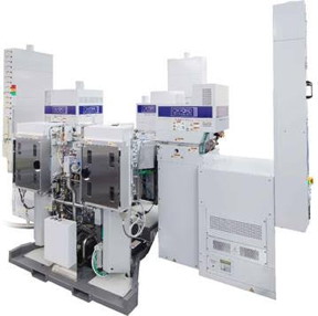
Oxford Instruments Plasma Technology's Atomic Layer Deposition (ALD) and Atomic Layer Etch (ALE) are critical process steps for GaN and SiC based devices to enable functionality and reliable device manufacturing. With the critical know-how and expertise gained over the last ten years in Wide Band Gap applications, Oxford Instruments Plasma Technology is perfectly placed to serve the technology leading Japanese production customers in these markets.
- Ends -
Issued for and on behalf of Oxford Instruments Plasma Technology
####
For more information, please click here
Contacts:Claire Critchell BA (Hons), ACIMMarketing Communications Manager
Oxford Instruments Plasma TechnologyNorth End, Yatton, Bristol BS49 4AP, UK Tel: +44 (0) 1934 837053
Copyright © Oxford Instruments Plasma Technology
If you have a comment, please Contact us.
Issuers of news releases, not 7th Wave, Inc. or Nanotechnology Now, are solely responsible for the accuracy of the content.
Bookmark:


News and information
![]() Scientists unravel 'Hall effect' mystery in search for next generation memory storage devices August 19th, 2022
Scientists unravel 'Hall effect' mystery in search for next generation memory storage devices August 19th, 2022
![]() Researchers design new inks for 3D-printable wearable bioelectronics: Potential uses include printing electronic tattoos for medical tracking applications August 19th, 2022
Researchers design new inks for 3D-printable wearable bioelectronics: Potential uses include printing electronic tattoos for medical tracking applications August 19th, 2022
Announcements
![]() Scientists unravel 'Hall effect' mystery in search for next generation memory storage devices August 19th, 2022
Scientists unravel 'Hall effect' mystery in search for next generation memory storage devices August 19th, 2022
![]() Researchers design new inks for 3D-printable wearable bioelectronics: Potential uses include printing electronic tattoos for medical tracking applications August 19th, 2022
Researchers design new inks for 3D-printable wearable bioelectronics: Potential uses include printing electronic tattoos for medical tracking applications August 19th, 2022
![]() Visualizing nanoscale structures in real time: Open-source software enables researchers to see materials in 3D while they're still on the electron microscope August 19th, 2022
Visualizing nanoscale structures in real time: Open-source software enables researchers to see materials in 3D while they're still on the electron microscope August 19th, 2022
Tools
![]() Atomic level deposition to extend Moore's law and beyond July 15th, 2022
Atomic level deposition to extend Moore's law and beyond July 15th, 2022
![]() New technology helps reveal inner workings of human genome June 24th, 2022
New technology helps reveal inner workings of human genome June 24th, 2022
![]() Snapshot measurement of single nanostructure's circular dichroism March 25th, 2022
Snapshot measurement of single nanostructure's circular dichroism March 25th, 2022
Alliances/Trade associations/Partnerships/Distributorships
![]() University of Illinois Chicago joins Brookhaven Lab's Quantum Center June 10th, 2022
University of Illinois Chicago joins Brookhaven Lab's Quantum Center June 10th, 2022
![]() University of Strathclyde and National University of Singapore to co-ordinate satellite quantum communications May 13th, 2022
University of Strathclyde and National University of Singapore to co-ordinate satellite quantum communications May 13th, 2022
![]() CEA and Startup C12 Join Forces to Develop Next-Generation Quantum Computers with Multi-Qubit Chips at Wafer Scale March 25th, 2022
CEA and Startup C12 Join Forces to Develop Next-Generation Quantum Computers with Multi-Qubit Chips at Wafer Scale March 25th, 2022
