
| Date | 23rd, Jan 2019 |
|---|
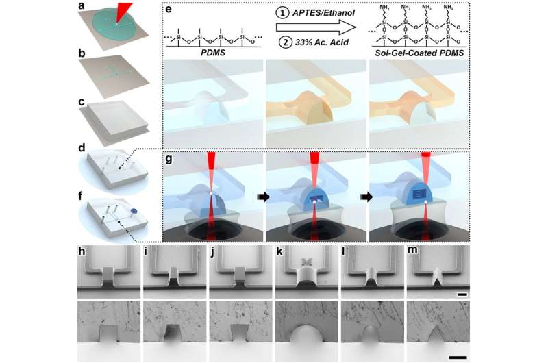
 Sol-gel-based in-situ direct laser writing (isDLW) concept. (a–g) Illustrations of the isDLW fabrication protocol for a microfluidic element printed inside a semi-ovular microchannel. (a) DLW of the channel mold structures. (b) Fabricated negative master mold. (c) Micromolding of poly(dimethylsiloxane) (PDMS). (d) Micromolded PDMS bonded to a glass substrate. (e) Acetic (Ac.) Acid-catalyzed sol-gel reaction for coating the PDMS microchannels with an adhesive layer of (3-Aminopropyl)triethoxysilane (APTES). (f) Vacuum loading of a liquid-phase photocurable material into the sol-gel-coated microchannels. (g) The “ceiling-to-floor” isDLW process. Focused femtosecond laser pulses (red) pass through an objective lens, immersion oil, glass substrate, and liquid-phase photomaterial to initiate spatially controlled photopolymerization (white) in a point-by-point, layer-by-layer methodology, ultimately producing a structure comprised of cured photomaterial (blue) that is fully sealed to the entire luminal surface of the sol-gel-coated microchannel. (h–m) Micrographs of (Top) DLW-printed negative master molds, and (Bottom) replicated PDMS profiles corresponding to distinct microchannel cross-sectional geometries: (h) rectangular (deep reactive-ion etching (DRIE) mimetic), (i) outward-tapered (positive-tone photoresist mimetic), (j) inward-tapered (negative-tone photoresist mimetic), (k) semi-circular, (l) semi-ovular, and (m) triangular (see also Supplementary Fig. S1). Scale bars = 100 μm. Credit: Scientific Reports
Engineers at the University of Maryland (UMD) have created the first 3-D-printed fluid circuit element so tiny that 10 could rest on the width of a human hair. The diode ensures fluids move in only a single direction—a critical feature for products like implantable devices that release therapies directly into the body.
The microfluidic diode also represents the first use of a 3-D nanoprinting strategy that breaks through previous cost and complexity barriers hindering advancements in areas from personalized medicine to drug delivery.
"Just as shrinking electric circuits revolutionized the field of electronics, the ability to dramatically reduce the size of 3-D printed microfluidic circuitry sets the stage for a new era in fields like pharmaceutical screening, medical diagnostics, and microrobotics," said Ryan Sochol, an assistant professor in mechanical engineering and bioengineering at UMD's A. James Clark School of Engineering.
Sochol, along with graduate students Andrew Lamont and Abdullah Alsharhan, outlined their new strategy in a paper published today in the open-access journal Nature: Scientific Reports.
Scientists have in recent years tapped into the emerging technology of 3-D nanoprinting to build medical devices and create "organ-on-a-chip" systems. But the complexity of pushing pharmaceuticals, nutrients, and other fluids into such small environments without leakage—and the costs of overcoming those complexities—made the technology impractical for most applications requiring precise fluid control.
Instead, researchers were limited to additive manufacturing technologies that print features significantly larger than the new UMD fluid diode.
"This really put a limit on how small your device could be," said Lamont, a bioengineering student who developed the approach and led the tests as part of his doctoral research. "After all, the microfluidic circuitry in your microrobot can't be larger than the robot itself."
What sets the Clark School team's strategy apart is its use of a process known as sol-gel, which allowed them to anchor their diode to the walls of a microscale channel printed with a common polymer. The diode's minute architecture was then printed directly inside of the channel—layer-by-layer, from the top of the channel down.
The result is a fully sealed, 3-D microfluidic diode created at a fraction of the cost and in less time than previous approaches.
The strong seal they achieved, which will protect the circuit from contamination and ensure any fluid pushed through the diode isn't released at the wrong time or place, was further strengthened by a reshaping of the microchannel walls.
"Where previous methods required researchers to sacrifice time and cost to build similar components, our approach allows us to essentially have our cake and eat it too," Sochol said. "Now, researchers can 3-D nanoprint complex fluidic systems faster, cheaper, and with less labor than ever before."
More information: Andrew C. Lamont et al. Geometric Determinants of In-Situ Direct Laser Writing, Scientific Reports (2019). DOI: 10.1038/s41598-018-36727-z
Citation: New 3-D nanoprinting strategy opens door to revolution in medicine, robotics (2019, January 23) retrieved 22 August 2022 from https://phys.org/news/2019-01-d-nanoprinting-strategy-door-revolution.html
This document is subject to copyright. Apart from any fair dealing for the purpose of private study or research, no part may be reproduced without the written permission. The content is provided for information purposes only.
