

| Date | 28th, Jan 2019 |
|---|
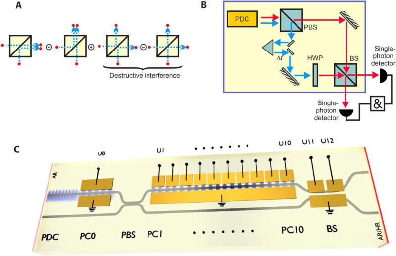 A schematic diagram of a miniaturized compact quantum circuit with active and accurate manipulation in LiNbO3 waveguides. (A) HOM bunching effect of indistinguishable photons in a beam splitter (BS). (B) Schematics of a typical HOM experiment using bulk optic components. All the functionalities in the yellow box are integrated into the chip. (C) Scheme of the integrated quantum optical chip with monolithically integrated PDC (parametric down conversion) source, electro-optic polarization converters (PCs), polarization beam splitter (PBS), and beam splitter (BS). The gray lines denote the Ti-indiffused waveguides. In the periodically poled PDC section, orthogonally polarized photon pairs (H and V) are generated. In the subsequent PC0, the complete conversion changes the polarization state of both photons from horizontal (H) to vertical (V) and vice versa via applying the control voltages U0. These photons are spatially separated by the PBS. Credit: Science Advances, doi: 10.1126/sciadv.aat1451
Physicists envision that the future of quantum computation networks will contain scalable, monolithic circuits, which include advanced functionalities on a single physical substrate. While substantial progress has already been made for a variety of applications on different platforms, the range of diverse photonic states that can be manipulated on demand on a single chip remain limited. This is specifically observed for dynamic time management in quantum devices.
In a recent study, now published in Science Advances, Kai-Hong Luo and co-workers demonstrate an electro-optic device, which included dynamic functionalities of photon pair generation, propagation and electro-optical path routing. The device contained voltage-controllable time delay approximating up to 12 picoseconds on a single Ti:LiNbO3 (titanium indiffused lithium niobate) waveguide chip.
As a proof-of-principle, the physicists at the interdisciplinary department of physics, optoelectronics and photonics demonstrated the Hong-Ou-Mandel interference with a visibility of more than 93 ± 1.8 percent. The chip developed by Luo et al. in the study allowed deliberate manipulation of photonic states by rotating the polarization. Experiments revealed that the physicists could exert full, flexible control on single-qubit operations by harnessing the complete potential of fast on-chip electro-optic modulation.
In the past decade, a range of materials has been used to develop optical circuits for quantum gates, quantum interference, quantum metrology, boson sampling and quantum walks. These circuits were developed on materials including glass, silicon nitride, silicon on insulator and silica on silicon. In comparison, the development of integrated photonic devices based on second-order nonlinearities has remained slow, despite the efficiency of exploiting the X(2) nonlinearities. Even with the success of tunable couplers and voltage-controlled phase shifters, the full potential of fast active electro-optic routing and rotation of polarized photons in quantum circuits remain to be harnessed.
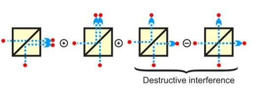 Schematic illustration of the HOM bunching effect of indistinguishable photons in a Beam Splitter. Credit: Science Advances, doi: 10.1126/sciadv.aat1451
The aim of Luo et al. was to demonstrate deliberate manipulation of photonic states via precise polarization and time regulation on a single quantum circuit device. For this, they focused on Hong-Ou-Mandel (HOM) interferences, among the most fundamental nonclassical experiments in quantum optics. HOM is at the heart of many quantum logic operations such as boson sampling, Bell-state measurement for quantum repeaters and the Knill, Laflamme and Milburn protocol for quantum computing. Nevertheless, a practical approach has not yet been produced on an integrated chip to contain all functionalities, and with the ability to manipulate quantum states on demand in the complete HOM experiment.
In the present study, Luo et al. offered an integrated electro-optic circuit design that could realize multiple operations on a single Ti:LiNbO3 waveguide chip. The integrated operations included:
Photon pair state generationPassive routingFast active polarization for qubit manipulationElectro-optic balanced switchingVariable time delay management.For all quantum logic operations, temporal synchronization of a manipulated state is a fundamental demand. As a result, fast and electro-optically controllable on-chip time delays are crucial inclusions for all quantum applications.
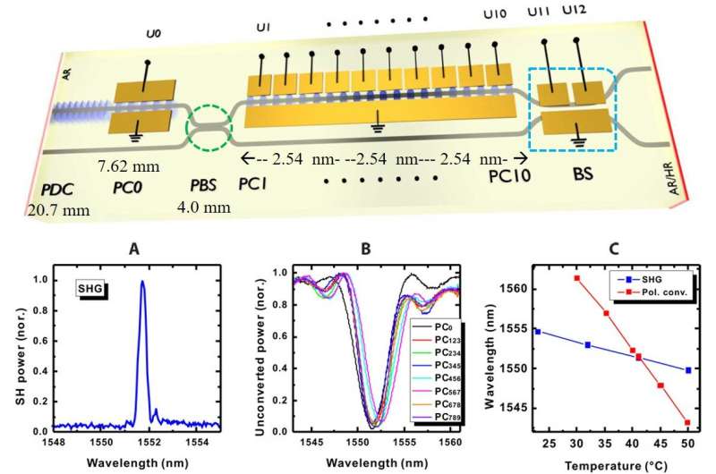 Upper panel: Schematic illustration of the integrated quantum optic chip with monolithic inclusions of a PDC source (20.7 mm), electro-optic PCs (7.62 mm), PBS, highlighted in green (4.0 mm), BS highlighted in blue, and a single element of the segmented converters (PC1 to PC10; 2.54 mm each). Lower panel: Classical characterization of the integrated circuit. A) Normalized power of the second harmonic (SH) wave generated in the PDC section with a poling period of ΔPDC = 9.04 µm as a function of the fundamental wavelength, which is from a tunable telecom laser with narrow bandwidth. (B) Spectral transmission characteristics of PC0 and the various triple combinations of the segmented PC (with a poling period of ΔPC = 21.4 µm). The scientists obtained the curves by launching broadband incoherent light in the telecom range and measuring the unconverted power behind a polarizer. The curves are normalized to a reference transmission spectrum obtained without conversion. (C) Temperature dependence of the two phase-matching processes (PDC and PC). Crossing of the two curves determines the optimum operation point, which is at T = 43.6°C and λ = 1551.7 nm. Credit: Science Advances, doi: 10.1126/sciadv.aat1451
The HOM effect can be experimentally produced by a beam splitter (BS). During the effect, two identical photons that enter a beam splitter from opposite input ports bunch together and leave at the same exit port. To demonstrate this quantum effect in an optical HOM experiment, the physicists generated photon pairs (signal and idler photons), and then spatially separated them with a polarization beam splitter (PBS). After polarization rotation and introducing a variable time delay between the photons, they were recombined at a symmetric beam splitter (BS) where quantum interference took place. For monolithic circuit fabrication, the physicists used the Ti:LiNbO3 platform, which exploited the strong X(2) nonlinearity during photon pair generation and electro-optic manipulation of the qubits.
Luo et al. then introduced the concept of birefringent electro-optic delay (BED) to overcome an intrinsic birefringent (double refraction of light) delay in the nonlinear medium. The method took advantage of the electro-optic polarization conversion and birefringence of the material itself to allow accurate on-chip time regulation.
The complex circuit design contained several different components that were already optimized as individual devices, the scientists fabricated the waveguides by Ti indiffusion for single-mode guiding in both polarizations. Importantly, in the monolithic on-chip electro-optic device, the relative delay between the signal and idler photons required adjustment via the segmented polarization controller. Another important criterion was the length of the entire device, which had to be kept as short as possible to fabricate homogenous structures.
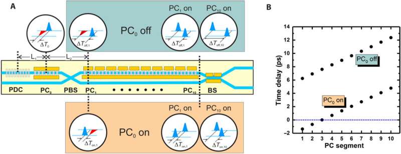 Illustration of the principle of the adjustable BED line. (A) The diagram shows the chip design together with some insets illustrating the temporal relation of the horizontally (red) and vertically (blue) polarized photon wave packets at different positions of the structure and for various configurations of the PCs. Case I: If PC0 is switched off, then the temporal walk-off increases along the structure. The time delay between the two photons can be varied, depending on which element of the segmented converter is switched on; however, the two photons will never arrive simultaneously at the BS (the HOM effect is not experimentally observed). Case II: If PC0 is switched on, then the originally horizontally polarized photon can overtake the other photon before they arrive at the segmented PC. A simultaneous arrival of the two photons at the BS can be achieved if a certain element of the segmented PC is addressed to fulfill the HOM effect. (B) Calculated time delay of the photons at the BS as a function of the element of the segmented PC, at which the final swapping of the polarization is performed. The diagram shows the result for the two cases of PC0 on and off. The dotted line indicates the time synchronization between the two polarized photons. The parameters used for the calculations are adapted to the geometry of the fabricated device—lengths of the PDC section (20.7 mm), PC0 (7.62 mm), the PBS section (4.0 mm), and a single element of the segmented converters (2.54 mm). A group index difference Δng = 0.0805 is derived from the Sellmeier equations of LiNbO3 (λ= 1551.7 nm). Credit: Science Advances, doi: 10.1126/sciadv.aat1451
The scientists generated photon pairs in the parametric down conversion (PDC) section (a nonlinear instant optical process that converted one photon of higher energy into a pair of photons), which contained the Ti-indiffused single-mode waveguide. For the HOM chip it was essential for the generated photon pairs to be degenerate. The degeneracy point could be tuned by varying the temperature, with a tuning slope approximating – 0.15 nm/0C. The device contained a specifically designed directional coupler to act as a polarization beam splitter (PBS) to spatially separate the orthogonally polarized photons.
Key elements of the BED system developed by Luo et al. included electro-optic polarization converters (PCs). These converters contained a periodically poled waveguide, with electrodes on each side. In the illustrated circuit design of the integrated quantum optical chip, the physicists placed the first PC (PC0) directly behind the PDC section. This was followed by a segmented PC10 (PC1 to PC10; containing 10 electro-optic elements) in one branch, after the polarization beam splitter (PBS) region. The beam splitter (BS), contained two waveguides separated by a 6 µm-wide gap.
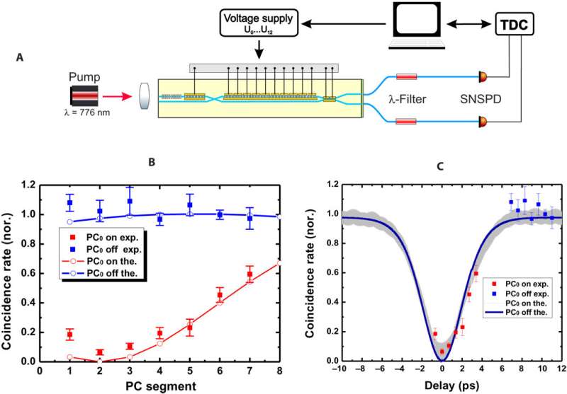 Experimental setup and quantum results. (A) Experimental setup for quantum characterization of the active HOM chip. A tunable narrowband continuous-wave pump laser around 776 nm is coupled into the channel with the PDC source. To avoid higher-order photon pair generation, the pump power is kept in the range of 100 µW. A temperature controller controls and stabilizes the previously determined temperature distribution of the sample. The two output ports from the chip are directly coupled into a pair of single-mode fibers via fiber-optical isolators to suppress the residual pump light and a 1.2-nm bandpass filter to suppress background photons, the transmitted photons are detected with superconducting nanowire detectors (SNSPDs) and time-to-digital converter (TDC). B) Experimental and simulated results of the normalized coincidence rate as a function of which triple of the segmented PC is driven. The blue data and curve are for PC0 off, while the red data and curve are for PC0 on. In the experiment, only seven triples of the segmented PC could be addressed because the electrode of PC10 was broken. Therefore, only 14 different delays were possible. (C) Experimental and simulated profiles of the HOM dip derived from the coincidence results shown in (B) and the corresponding calculated time delay. Credit: Science Advances, doi: 10.1126/sciadv.aat1451
The scientists illustrated the working principle of the adjustable BED system to show how the calculated group index difference ∆ng caused a temporal walk-off between a pair of photons. Depending on the off/on status of PC0, the polarization states (horizontal or vertical) of the photon pair either remain unchanged or swapped to spatially separate at the PBS to demonstrate the HOM effect.
When PC0 was switched on, polarizations of the photon pair swapped to simultaneously arrive at the segmented PC (with 10 electro-optic segments: PC1 to PC10). The scientists showed how the simultaneous arrival of two photons at the beam splitter (BS) could be experimentally achieved. Luo et al. also showed that the relative time delay between the two photons at the input ports of the beam splitter could be finely adjusted between ~ 1.3 ps to more than 12 ps for dynamic time management on the device.
The scientists implemented the proposed measurement setup of the entire quantum experiment in the lab by including an external pump, fiber filters and detection units. To confirm that two-photon interference of the study is in the quantum regime for two perfectly identical photons, the coincidence count rates (used to test quantum entanglement) between the two waveguide outputs detected should drop to zero. Additionally, to prove quantum interference, the drop (dip) of coincidences should have a visibility beyond the classically expected value of 50 percent. Luo et al. calculated the visibility of the HOM interference at 93.5 ± 1.8 percent, a value significantly higher than the classical limit, verifying the quantum nature of the on-chip two-photon interference.
In this way, the physicists amply demonstrated a quantum electro-optic circuit that could actively manipulate photon states for adjustable time management within a monolithically integrated device. They used a two-photon HOM chip with a source of photon pairs for active polarization manipulation. The work creates a new approach for integrated electro-optic circuits and opens a door to harness the tremendous potential of qubit manipulation in Ti:LiNbO3, for quantum applications. The device paves the way toward future quantum logic operations, hyperentanglement and ultrafast processing seen with fiber-optics, yet rarely used in quantum optics.
More information: Kai-Hong Luo et al. Nonlinear integrated quantum electro-optic circuits, Science Advances (2019). DOI: 10.1126/sciadv.aat1451
Andrea Crespi et al. Anderson localization of entangled photons in an integrated quantum walk, Nature Photonics (2013). DOI: 10.1038/nphoton.2013.26
Damien Bonneau et al. Fast Path and Polarization Manipulation of Telecom Wavelength Single Photons in Lithium Niobate Waveguide Devices, Physical Review Letters (2012). DOI: 10.1103/PhysRevLett.108.053601
Kai-Hong Luo et al. Monolithically Integrated Hong-Ou-Mandel Experiment in LiNbO3, Conference on Lasers and Electro-Optics (2018). DOI: 10.1364/CLEO_QELS.2018.FM1G.3
C. K. Hong et al. Experimental realization of a localized one-photon state, Physical Review Letters (2002). DOI: 10.1103/PhysRevLett.56.58
© 2019 Science X Network
Citation: Nonlinear integrated quantum electro-optic circuits (2019, January 28) retrieved 22 August 2022 from https://phys.org/news/2019-01-nonlinear-quantum-electro-optic-circuits.html
This document is subject to copyright. Apart from any fair dealing for the purpose of private study or research, no part may be reproduced without the written permission. The content is provided for information purposes only.
