| Date | 2nd, Feb 2019 |
|---|
Home > Press > Large, stable pieces of graphene produced with unique edge pattern: Breakthrough in graphene research
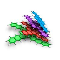 The much sought-after zigzag pattern can be found either in staggered rows of honeycombs (blue and purple) or four-limbed stars surrounding a central point of four graphene honeycombs (red and green). (Image: FAU/Konstantin Amsharov)
Abstract: Graphene is a promising material for use in nanoelectronics. Its electronic properties depend greatly, however, on how the edges of the carbon layer are formed. Zigzag patterns are particularly interesting in this respect, but until now it has been virtually impossible to create edges with a pattern like this. Chemists and physicists at FAU have now succeeded in producing stable nanographene with a zigzag edge. Not only that, the method they used was even comparatively simple. Their research, conducted within the framework of collaborative research centre 953 - Synthetic Carbon Allotropes funded by the German Research Foundation (DFG), has now been published in the journal Nature Communications.
Erlangen, Germany | Posted on February 1st, 2019
Bay, fjord, cove, armchair and zigzag - when chemists use terms such as these, it is clear that they are referring to nanographene. More specifically, the shape taken by the edges of nanographene, i.e. small fragments of graphene. Graphene consists of a single-layered carbon structure, where each carbon atom is surrounded by three others. This creates a pattern reminiscent of a honeycomb, with atoms in each of the corners. Nanographene is a promising candidate for use in the field of microelectronics, taking over from silicon which is used today and bringing microelectronics down to the nano scale.
The electronic properties of the material depend greatly on its shape, size and above all, periphery, in other words how the edges are structured. A zigzag periphery is particularly suitable, as in this case the electrons, which act as charge carriers, are more mobile than in other edge structures. This means that using pieces of zigzag-shaped graphene in nanoelectronic components may allow higher frequencies for switches.
The problem currently faced by materials scientists who want to research only zigzag nanographene is that this form makes the compounds rather unstable, and unable to be produced in a controlled manner. This is a prerequisite, however, if the electronic properties are to be investigated in detail.
The team of researchers led by PD Dr. Konstantin Amsharov from the Chair of Organic Chemistry II have now succeeded in doing just that. Not only have they discovered a straightforward method for synthesising zigzag nanographene, their procedure delivers a yield of close to one hundred percent and is suitable for large scale production. They have already produced a technically relevant quantity in the laboratory.
First of all, the FAU researchers produce preliminary molecules, which they then fitt together in a honeycomb formation over several cycles, in a process known as cyclisation. In the end, graphene fragments are produced from staggered rows of honeycombs or four-limbed stars surrounding a central point of four graphene honeycombs, with the sought-after zigzag pattern to their edges. Why is this method able to produce stable zigzag nanographene? The explanation lies in the fact that the product crystallises directly even during synthesis. In their solid state, the molecules are not in contact with oxygen. In solution, however, oxidation causes the structures to disintegrate quickly.
This approach allows scientists to produce large pieces of graphene, whilst maintaining control over their shape and periphery. This breakthrough in graphene research means that scientists should soon be able to produce and research a variety of interesting nanographene structures, a crucial step towards finally being able to use the material in nanoelectronic components.
####
For more information, please click here
Contacts:FAU Press Office
49-913-185-70229
Copyright © UNIVERSITY OF ERLANGEN-NUREMBERG
If you have a comment, please Contact us.
Issuers of news releases, not 7th Wave, Inc. or Nanotechnology Now, are solely responsible for the accuracy of the content.
Bookmark:


News and information
![]() Scientists unravel 'Hall effect' mystery in search for next generation memory storage devices August 19th, 2022
Scientists unravel 'Hall effect' mystery in search for next generation memory storage devices August 19th, 2022
![]() Researchers design new inks for 3D-printable wearable bioelectronics: Potential uses include printing electronic tattoos for medical tracking applications August 19th, 2022
Researchers design new inks for 3D-printable wearable bioelectronics: Potential uses include printing electronic tattoos for medical tracking applications August 19th, 2022
2 Dimensional Materials
![]() Buckyballs on gold are less exotic than graphene July 22nd, 2022
Buckyballs on gold are less exotic than graphene July 22nd, 2022
![]() Controlled synthesis of crystal flakes paves path for advanced future electronics June 17th, 2022
Controlled synthesis of crystal flakes paves path for advanced future electronics June 17th, 2022
Graphene/ Graphite
![]() Buckyballs on gold are less exotic than graphene July 22nd, 2022
Buckyballs on gold are less exotic than graphene July 22nd, 2022
![]() A novel graphene based NiSe2 nanocrystalline array for efficient hydrogen evolution reaction July 15th, 2022
A novel graphene based NiSe2 nanocrystalline array for efficient hydrogen evolution reaction July 15th, 2022
Possible Futures
![]() New chip ramps up AI computing efficiency August 19th, 2022
New chip ramps up AI computing efficiency August 19th, 2022
![]() Rice team eyes cells for sophisticated data storage: National Science Foundation backs effort to turn living cells into equivalent of computer RAM August 19th, 2022
Rice team eyes cells for sophisticated data storage: National Science Foundation backs effort to turn living cells into equivalent of computer RAM August 19th, 2022
Chip Technology
![]() New chip ramps up AI computing efficiency August 19th, 2022
New chip ramps up AI computing efficiency August 19th, 2022
![]() Scientists unravel 'Hall effect' mystery in search for next generation memory storage devices August 19th, 2022
Scientists unravel 'Hall effect' mystery in search for next generation memory storage devices August 19th, 2022
![]() Researchers design new inks for 3D-printable wearable bioelectronics: Potential uses include printing electronic tattoos for medical tracking applications August 19th, 2022
Researchers design new inks for 3D-printable wearable bioelectronics: Potential uses include printing electronic tattoos for medical tracking applications August 19th, 2022
Nanoelectronics
![]() Atomic level deposition to extend Moore's law and beyond July 15th, 2022
Atomic level deposition to extend Moore's law and beyond July 15th, 2022
![]() Controlled synthesis of crystal flakes paves path for advanced future electronics June 17th, 2022
Controlled synthesis of crystal flakes paves path for advanced future electronics June 17th, 2022
![]() Eyebrow-raising: Researchers reveal why nanowires stick to each other February 11th, 2022
Eyebrow-raising: Researchers reveal why nanowires stick to each other February 11th, 2022
Discoveries
![]() Scientists unravel 'Hall effect' mystery in search for next generation memory storage devices August 19th, 2022
Scientists unravel 'Hall effect' mystery in search for next generation memory storage devices August 19th, 2022
![]() Researchers design new inks for 3D-printable wearable bioelectronics: Potential uses include printing electronic tattoos for medical tracking applications August 19th, 2022
Researchers design new inks for 3D-printable wearable bioelectronics: Potential uses include printing electronic tattoos for medical tracking applications August 19th, 2022
![]() Visualizing nanoscale structures in real time: Open-source software enables researchers to see materials in 3D while they're still on the electron microscope August 19th, 2022
Visualizing nanoscale structures in real time: Open-source software enables researchers to see materials in 3D while they're still on the electron microscope August 19th, 2022
Materials/Metamaterials
![]() Strain-sensing smart skin ready to deploy: Nanotube-embedded coating detects threats from wear and tear in large structures July 15th, 2022
Strain-sensing smart skin ready to deploy: Nanotube-embedded coating detects threats from wear and tear in large structures July 15th, 2022
![]() New protocol for assessing the safety of nanomaterials July 1st, 2022
New protocol for assessing the safety of nanomaterials July 1st, 2022
![]() Nanotubes: a promising solution for advanced rubber cables with 60% less conductive filler June 1st, 2022
Nanotubes: a promising solution for advanced rubber cables with 60% less conductive filler June 1st, 2022
Announcements
![]() Scientists unravel 'Hall effect' mystery in search for next generation memory storage devices August 19th, 2022
Scientists unravel 'Hall effect' mystery in search for next generation memory storage devices August 19th, 2022
![]() Researchers design new inks for 3D-printable wearable bioelectronics: Potential uses include printing electronic tattoos for medical tracking applications August 19th, 2022
Researchers design new inks for 3D-printable wearable bioelectronics: Potential uses include printing electronic tattoos for medical tracking applications August 19th, 2022
![]() Visualizing nanoscale structures in real time: Open-source software enables researchers to see materials in 3D while they're still on the electron microscope August 19th, 2022
Visualizing nanoscale structures in real time: Open-source software enables researchers to see materials in 3D while they're still on the electron microscope August 19th, 2022
Interviews/Book Reviews/Essays/Reports/Podcasts/Journals/White papers/Posters
![]() Scientists unravel 'Hall effect' mystery in search for next generation memory storage devices August 19th, 2022
Scientists unravel 'Hall effect' mystery in search for next generation memory storage devices August 19th, 2022
![]() Researchers design new inks for 3D-printable wearable bioelectronics: Potential uses include printing electronic tattoos for medical tracking applications August 19th, 2022
Researchers design new inks for 3D-printable wearable bioelectronics: Potential uses include printing electronic tattoos for medical tracking applications August 19th, 2022
![]() Visualizing nanoscale structures in real time: Open-source software enables researchers to see materials in 3D while they're still on the electron microscope August 19th, 2022
Visualizing nanoscale structures in real time: Open-source software enables researchers to see materials in 3D while they're still on the electron microscope August 19th, 2022
