When these materials are made, defects can occur at the points known as grain boundaries, where different crystals meet. In conventional semiconductors, these defects can decrease electrical conductivity and the solar energy-to-electricity conversion efficiency. However, in lead-halide perovskites, there are differing experimental reports on the impact of defects caused by grain boundaries.
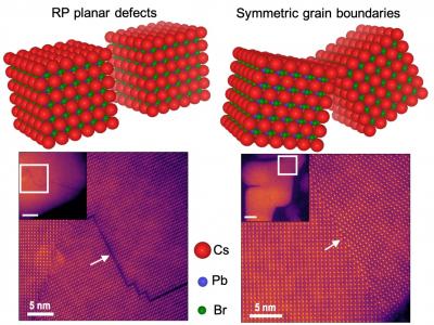 Using atomic-resolution electron microscopy, Arashdeep Singh Thind, a graduate student in Rohan Mishra’s lab, studied grain boundaries in crystals (see arrows). Courtesy of Washington University in St. Louis.
In silicon semiconductors, grain boundaries can wreak havoc, but in lead-halide perovskites, they may not be harmful and could even be beneficial. Their impact depends on the concentration of the halide ions. “If you grow the crystals in a halide-poor environment, then the grain boundaries are terrible for performance,” professor Rohan Mishra said. “But if you can grow them or anneal (heat and recombine) them in a halide-rich atmosphere, the grain boundaries are fine.”
Using atomic-resolution electron microscopy, Arashdeep Singh Thind, a graduate student in Rohan Mishra’s lab, studied grain boundaries in crystals (see arrows). Courtesy of Washington University in St. Louis.
In silicon semiconductors, grain boundaries can wreak havoc, but in lead-halide perovskites, they may not be harmful and could even be beneficial. Their impact depends on the concentration of the halide ions. “If you grow the crystals in a halide-poor environment, then the grain boundaries are terrible for performance,” professor Rohan Mishra said. “But if you can grow them or anneal (heat and recombine) them in a halide-rich atmosphere, the grain boundaries are fine.”
Researchers at Oak Ridge National Lab examined the atomic structure of the grain boundaries using an electron microscope. A former research scientist in Mishra’s lab, now at Southern University of Science and Technology in Shenzhen, China, then used quantum-mechanical calculations to understand the electronic properties of the grain boundaries.
The team also looked at another type of planar fault known as a Ruddlesden-Popper fault, in which the planes of crystals stack incorrectly. Using quantum mechanical calculations, the researchers found that a large density of stacking faults could help enable bright optical emission from large and more stable nanoparticles of certain lead-halide perovskites, potentially leading to LEDs with longer lifetimes. “The challenge for experimentalists is to engineer stacking faults at periodic distances,” Mishra said.
In related research, published in ACS Applied Nano Materials (https://pubs.acs.org/doi/10.1021/acsanm.8b01298) on Oct. 16, 2018, Mishra’s team worked with University of Missouri-Columbia researchers who found a new chemical route for promoting the growth of lead-halide perovskites with a high density of stacking faults. By removing surface ligands, smaller lead-halide perovskite nanocrystals fused and grew from about 8 nm to 60 nm in 48 hours. These new nanocrystals demonstrated significantly enhanced optical properties due to the stacking faults formed during the fusion process. In addition, the new nanocrystals were more stable when exposed to light, had sharper emission lines, and had a higher quantum yield than the original lead-halide perovskite crystals.
The team will use its findings to search for alternatives to using lead in solar cells. Mishra is studying whether a nontoxic element — bismuth, lead’s neighbor on the periodic table — is a safer and equally efficient substitute for lead in perovskites.
The research was published in Advanced Materials (https://doi.org/10.1002/adma.201805047).
