| Date | 1st, Jun 2018 |
|---|
Home > Press > Building nanomaterials for next-generation computing: Scientists recently developed a blueprint to fabricate new nanoheterostructures using 2D materials
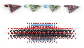 Nanoscientists at Northwestern University have developed a blueprint to fabricate new heterostructures from different types of 2-D materials. The researchers describe their blueprint in the Journal of Applied Physics. In this image: Top: Vertical MoSe2-WSe2 heterostructure, radial MoS2-WS2 heterostructure, hybrid MoS2-WS2 heterostructure and Mose2-WSe2 alloy building block representations and crystal structure models Bottom: Vertical MoSe2-WSe2 heterostructure crystal structure model
CREDIT
Cain, Hanson and Dravid
Nanoscientists at Northwestern University have developed a blueprint to fabricate new heterostructures from different types of 2-D materials. The researchers describe their blueprint in the Journal of Applied Physics. In this image: Top: Vertical MoSe2-WSe2 heterostructure, radial MoS2-WS2 heterostructure, hybrid MoS2-WS2 heterostructure and Mose2-WSe2 alloy building block representations and crystal structure models Bottom: Vertical MoSe2-WSe2 heterostructure crystal structure model
CREDIT
Cain, Hanson and Dravid
Abstract: Nanoscientists at Northwestern University have developed a blueprint to fabricate new heterostructures from different types of 2-D materials. 2-D materials are single atom layers that can be stacked together like "nano-interlocking building blocks." Materials scientists and physicists are excited about the properties of 2-D materials and their potential applications. The researchers describe their blueprint in the Journal of Applied Physics, from AIP Publishing.
Washington, DC | Posted on June 1st, 2018
"We've outlined an easy, deterministic and readily deployable way to stack and stitch these individual layers into orders not seen in nature," said Jeffrey Cain, an author on the paper who was formerly at Northwestern University but is now at Lawrence Berkeley National Laboratory and the University of California.
Cain explained that for nanoscientists, "the dream" is to combine 2-D materials in any order and collate a library of these heterostructures with their documented properties. Scientists can then select appropriate heterostructures from the library for their desired applications. For instance, the computer industry is trying to make transistors smaller and faster to increase computing power. A nanoscale semiconductor with favorable electronic properties could be used to make transistors in next-generation computers.
So far, nanoscientists have lacked clear methods for fabricating heterostructures, and have not yet been able to develop this library. In this work, the scientists looked to solve these fabrication issues. After identifying trends in the literature, they tested different conditions to map out the different parameters required to grow specific heterostructures from four types of 2-D materials: molybdenum disulfide and diselenide, and tungsten disulfide and diselenide. To fully characterize the atomically thin final products, the scientists used microscopy and spectrometry techniques.
The group was inspired by the science of time-temperature-transformation diagrams in classical materials, which maps out heating and cooling profiles to generate precise metallic microstructures. Based on this method, the researchers packaged their findings into one diagrammatic technique -- the Time-Temperature-Architecture Diagram.
"People had previously written papers for specific morphologies, but we have unified it all and enabled the generation of these morphologies with one technique," Cain said.
The unified Time-Temperature-Architecture Diagrams provide directions for the exact conditions required to generate numerous heterostructure morphologies and compositions. Using these diagrams, the researchers developed a unique library of nanostructures with physical properties of interest to physicists and materials scientists. The Northwestern University scientists are now examining the behaviors displayed by some materials in their library, like the electron flow across the stitched junctions between materials.
The researchers hope that their blueprint design will be useful for heterostructure fabrication beyond the first four materials. "Our specific diagrams would need revisions in the context of each new material, but we think that this idea is applicable and extendable to other material systems," Cain said.
####
About American Institute of PhysicsJournal of Applied Physics is an influential international journal publishing significant new experimental and theoretical results of applied physics research. See http://jap.aip.org .
For more information, please click here
Contacts:Julia Majors
301-209-3090
Copyright © American Institute of Physics
If you have a comment, please Contact us.
Issuers of news releases, not 7th Wave, Inc. or Nanotechnology Now, are solely responsible for the accuracy of the content.
Bookmark:


News and information
![]() Scientists unravel 'Hall effect' mystery in search for next generation memory storage devices August 19th, 2022
Scientists unravel 'Hall effect' mystery in search for next generation memory storage devices August 19th, 2022
![]() Researchers design new inks for 3D-printable wearable bioelectronics: Potential uses include printing electronic tattoos for medical tracking applications August 19th, 2022
Researchers design new inks for 3D-printable wearable bioelectronics: Potential uses include printing electronic tattoos for medical tracking applications August 19th, 2022
![]() Visualizing nanoscale structures in real time: Open-source software enables researchers to see materials in 3D while they're still on the electron microscope August 19th, 2022
Visualizing nanoscale structures in real time: Open-source software enables researchers to see materials in 3D while they're still on the electron microscope August 19th, 2022
Laboratories
2 Dimensional Materials
![]() Buckyballs on gold are less exotic than graphene July 22nd, 2022
Buckyballs on gold are less exotic than graphene July 22nd, 2022
![]() Controlled synthesis of crystal flakes paves path for advanced future electronics June 17th, 2022
Controlled synthesis of crystal flakes paves path for advanced future electronics June 17th, 2022
![]() Solving the puzzle of 2D disorder: An interdisciplinary team developed a new method to characterize disorder in 2D materials June 17th, 2022
Solving the puzzle of 2D disorder: An interdisciplinary team developed a new method to characterize disorder in 2D materials June 17th, 2022
Hardware
![]() A Carbon Nanotube Microprocessor Mature Enough to Say Hello: Three new breakthroughs make commercial nanotube processors possible March 2nd, 2020
A Carbon Nanotube Microprocessor Mature Enough to Say Hello: Three new breakthroughs make commercial nanotube processors possible March 2nd, 2020
![]() Powering the future: Smallest all-digital circuit opens doors to 5 nm next-gen semiconductor February 11th, 2020
Powering the future: Smallest all-digital circuit opens doors to 5 nm next-gen semiconductor February 11th, 2020
![]() Do you Kyoto? World-leading companies share their approaches to environmentally friendly business at NAUM'19 October 14th, 2019
Do you Kyoto? World-leading companies share their approaches to environmentally friendly business at NAUM'19 October 14th, 2019
Possible Futures
![]() New chip ramps up AI computing efficiency August 19th, 2022
New chip ramps up AI computing efficiency August 19th, 2022
![]() Rice team eyes cells for sophisticated data storage: National Science Foundation backs effort to turn living cells into equivalent of computer RAM August 19th, 2022
Rice team eyes cells for sophisticated data storage: National Science Foundation backs effort to turn living cells into equivalent of computer RAM August 19th, 2022
Chip Technology
![]() New chip ramps up AI computing efficiency August 19th, 2022
New chip ramps up AI computing efficiency August 19th, 2022
![]() Scientists unravel 'Hall effect' mystery in search for next generation memory storage devices August 19th, 2022
Scientists unravel 'Hall effect' mystery in search for next generation memory storage devices August 19th, 2022
![]() Researchers design new inks for 3D-printable wearable bioelectronics: Potential uses include printing electronic tattoos for medical tracking applications August 19th, 2022
Researchers design new inks for 3D-printable wearable bioelectronics: Potential uses include printing electronic tattoos for medical tracking applications August 19th, 2022
Nanoelectronics
![]() Atomic level deposition to extend Moore's law and beyond July 15th, 2022
Atomic level deposition to extend Moore's law and beyond July 15th, 2022
![]() Controlled synthesis of crystal flakes paves path for advanced future electronics June 17th, 2022
Controlled synthesis of crystal flakes paves path for advanced future electronics June 17th, 2022
![]() Eyebrow-raising: Researchers reveal why nanowires stick to each other February 11th, 2022
Eyebrow-raising: Researchers reveal why nanowires stick to each other February 11th, 2022
Materials/Metamaterials
![]() Strain-sensing smart skin ready to deploy: Nanotube-embedded coating detects threats from wear and tear in large structures July 15th, 2022
Strain-sensing smart skin ready to deploy: Nanotube-embedded coating detects threats from wear and tear in large structures July 15th, 2022
![]() New protocol for assessing the safety of nanomaterials July 1st, 2022
New protocol for assessing the safety of nanomaterials July 1st, 2022
![]() Nanotubes: a promising solution for advanced rubber cables with 60% less conductive filler June 1st, 2022
Nanotubes: a promising solution for advanced rubber cables with 60% less conductive filler June 1st, 2022
Announcements
![]() Scientists unravel 'Hall effect' mystery in search for next generation memory storage devices August 19th, 2022
Scientists unravel 'Hall effect' mystery in search for next generation memory storage devices August 19th, 2022
![]() Researchers design new inks for 3D-printable wearable bioelectronics: Potential uses include printing electronic tattoos for medical tracking applications August 19th, 2022
Researchers design new inks for 3D-printable wearable bioelectronics: Potential uses include printing electronic tattoos for medical tracking applications August 19th, 2022
![]() Visualizing nanoscale structures in real time: Open-source software enables researchers to see materials in 3D while they're still on the electron microscope August 19th, 2022
Visualizing nanoscale structures in real time: Open-source software enables researchers to see materials in 3D while they're still on the electron microscope August 19th, 2022
Interviews/Book Reviews/Essays/Reports/Podcasts/Journals/White papers/Posters
![]() Scientists unravel 'Hall effect' mystery in search for next generation memory storage devices August 19th, 2022
Scientists unravel 'Hall effect' mystery in search for next generation memory storage devices August 19th, 2022
![]() Researchers design new inks for 3D-printable wearable bioelectronics: Potential uses include printing electronic tattoos for medical tracking applications August 19th, 2022
Researchers design new inks for 3D-printable wearable bioelectronics: Potential uses include printing electronic tattoos for medical tracking applications August 19th, 2022
![]() Visualizing nanoscale structures in real time: Open-source software enables researchers to see materials in 3D while they're still on the electron microscope August 19th, 2022
Visualizing nanoscale structures in real time: Open-source software enables researchers to see materials in 3D while they're still on the electron microscope August 19th, 2022
