The approach exploits strain at highly spatially localized and spectrally well-separated defect emission sites, or tips, in the 750- to 800-nm regime in a tungsten/selenium film. The team synthesized the film through chemical vapor deposition using a multistep, diffusion-mediated gas source.
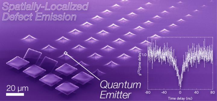 An innovative method for controlling single-photon emission for specific locations in 2D materials could offer a path toward all-optical quantum computers and other quantum technologies. This image shows a false-color scanning electron micrograph of the array used to create and place single-photon sources in epitaxial tungsten diselenide. Inset shows the Hanbury-Brown Twiss interferometry measurement proving quantum emission. Courtesy of Michael Pettes/Los Alamos National Laboratory.
To separate the effects of mechanical strain from the substrate or dielectric-environment-induced changes in the electronic structure, the researchers created arrays of silicon dioxide tips with spatial dimensions on the order of 10 μm. The researchers used bending based on the small (about 4 nm) radius of the tips to impart electronic localization effects through morphology alone. The resulting strain was enough to change the electronic structure, but only at the tips. When the researchers transferred the film onto an array of silicon dioxide tips, they observed about an 87% yield of localized emission sites on the tips.
An innovative method for controlling single-photon emission for specific locations in 2D materials could offer a path toward all-optical quantum computers and other quantum technologies. This image shows a false-color scanning electron micrograph of the array used to create and place single-photon sources in epitaxial tungsten diselenide. Inset shows the Hanbury-Brown Twiss interferometry measurement proving quantum emission. Courtesy of Michael Pettes/Los Alamos National Laboratory.
To separate the effects of mechanical strain from the substrate or dielectric-environment-induced changes in the electronic structure, the researchers created arrays of silicon dioxide tips with spatial dimensions on the order of 10 μm. The researchers used bending based on the small (about 4 nm) radius of the tips to impart electronic localization effects through morphology alone. The resulting strain was enough to change the electronic structure, but only at the tips. When the researchers transferred the film onto an array of silicon dioxide tips, they observed about an 87% yield of localized emission sites on the tips.According to the researchers, the 2D, tungsten/selenium thin films are scalable, making them potentially useful in processes to manufacture quantum technologies. Single-photon generation is a requirement for all-optical quantum computing and key distribution in quantum communications, and it is crucial for advancing quantum information technologies.
“While more research is needed to fully understand the role of mechanical deformation in creating these quantum emission sites, we may enable a route to control quantum optical properties by using strain,” researcher Michael Pettes said. “These single-photon sources form the basis for photonics-based, all-optical quantum computing schemes.”
Engineering of quantum emission in 2D materials is still in a very early stage, the researchers said. While studies have observed single photons originating from defect structures in these materials, previous work has suggested that nonuniform strain fields might govern the effect. The mechanism responsible for this phenomenon remains unclear and is the focus of ongoing work at Los Alamos National Laboratory.
The research was published in Applied Physics Letters (https://doi.org/10.1063/1.5091779).
