
| Date | 27th, Jun 2019 |
|---|
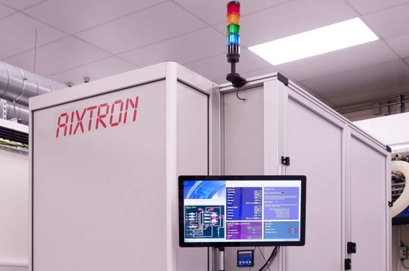
 AIXTRON's new 'Neutron' roll to roll system for the production of graphene. Credit: AIXTRON / Graphene Flagship
Today, Graphene Flagship partner AIXTRON showcased two systems that enable cost effective graphene production for applications in consumer electronics, sensors and photonic applications.
Graphene Flagship partner AIXTRON introduced results from two of its systems that enable the large-scale production of graphene through chemical vapour deposition (CVD). The Neutron is a roll-to-roll system capable of depositing large areas of graphene on metal foils under ambient conditions; the CCS 2-D system enables wafer-scale production of graphene on insulating wafers, a breakthrough that will speed up the development of new graphene electronics. To demonstrate the cost-effective nature of the graphene produced, AIXTRON distributed samples at the Industrial Forum.
The innovative Neutron system has a capacity of up to 20,000 square meters of graphene per year; this is around 200 times the production capacity of typical reactors in use today. Alex Jouvray, programme manager at AIXTRON and Graphene Flagship work package leader for production, says, "Neutron is the product that resulted from of over three years of R&D, which included the demonstration of roll-to-roll graphene growth during the first stages of the Graphene Flagship project."
Neutron brings the production of large areas of graphene beyond academic circles and to the factory floor. "The foil that is coated with graphene enters and exits the Neutron system under ambient conditions," explains Jouvray. "Since it doesn't need a vacuum, the Neutron can be easily placed inline at graphene manufacturing plants," he adds. Large-area monolayer graphene produced using this novel technique could lead to applications in transparent conductors, wearable devices, and coatings. "Moreover, it's economical," adds Jouvray. "With Neutron, we are able to bring the cost of a square meter of graphene CVD films down by two orders of magnitude," he explains. "It's a game-changer."
The versatile CCS system targets semiconductor applications. Here, there are stringent contamination requirements; usually, graphene needs to be grown on metallic surfaces and foils, which, being non-flat, are challenging to handle in the semiconductor industry and contain metal contamination that requires further cleaning steps before the material can enter a fab. During the first years of the Graphene Flagship project, together with the group of Camilla Coletti at Graphene Flagship partner Istituto Italiano di Tecnologia (IIT), AIXTRON scaled the growth of graphene on insulators to full wafer-scale on its CCS 2-D reactor, which can accommodate 2-inch up to 8-inch wafers. The wafers exhibit low contamination levels that meet the requirements of semiconductor fabs directly after growth. Camilla Coletti comments that "such tremendous progress is only possible thanks to the Graphene Flagship project which brings together top scientists from academia and engineers from a world-leading equipment company." The system is also capable of large-scale production of other layered materials, such as boron nitride or transition metal dichalcogenides.
Kari Hjelt, Head of Innovation of the Graphene Flagship believes that "these systems developed by AIXTRON show how our investment into prototypes during the first years of the Graphene Flagship are leading to products that enable mass production of graphene by chemical vapour deposition." He adds, "these discoveries open up thousands of possibilities beyond graphene, the arrival of wafers featuring other layered materials, or even sandwich heterostructures are just around the corner," concludes Hjelt.
Andrea C. Ferrari, Science and Technology Officer of the Graphene Flagship and Chair of its Management Panel added that "the ultimate aim of the Graphene Flagship is to bring graphene and related layered materials from the lab to the factory floor. To take these new materials to the traditional semiconductor fabs, which is key to achieve their widespread application in consumer electronics, photonics and sensors, industrial tools capable of large area, large rate and low-cost manufacturing of graphene and related materials are needed."
"With these systems," adds Ferrari, "Graphene Flagship Partner AIXTRON leads the way fostering the new market opportunities that these new materials open. The ability to produce large scale graphene viably is of particular importance as the Graphene Flagship gears up to launch the first Graphene Foundry. Moreover, these products are a cornerstone in the innovation and technology roadmap of the Graphene Flagship, and shows that we are set to achieve the ambitious goals for our first ten years."
Provided by Graphene Flagship
Citation: Cost-effective, large scale graphene with AIXTRON systems (2019, June 27) retrieved 5 July 2022 from https://phys.org/news/2019-06-cost-effective-large-scale-graphene-aixtron.html
This document is subject to copyright. Apart from any fair dealing for the purpose of private study or research, no part may be reproduced without the written permission. The content is provided for information purposes only.
