| Date | 20th, Jul 2019 |
|---|
Home > Press > Limitation exposed in promising quantum computing material: Metallic surfaces no longer protected as topological insulators become thinner
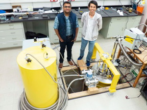 Vikram Deshpande, assistant professor in the Department of Physics & Astronomy (left) and doctoral candidate Su Kong Chong (right) stand in the "coolest lab on campus." Deshpande leads a lab that can cool topological materials down to just a few fractions of a degree above absolute zero at -273.15�C (-459.67�F). It is literally the coldest laboratory on campus.
CREDIT
Lisa Potter/University of Utah
Vikram Deshpande, assistant professor in the Department of Physics & Astronomy (left) and doctoral candidate Su Kong Chong (right) stand in the "coolest lab on campus." Deshpande leads a lab that can cool topological materials down to just a few fractions of a degree above absolute zero at -273.15�C (-459.67�F). It is literally the coldest laboratory on campus.
CREDIT
Lisa Potter/University of Utah
Abstract: Quantum computers promise to perform operations of great importance believed to be impossible for our technology today. Current computers process information via transistors carrying one of two units of information, either a 1 or a 0. Quantum computing is based on the quantum mechanical behavior of the logic unit. Each quantum unit, or "qubit," can exist in a quantum superposition rather than taking discrete values. The biggest hurdles to quantum computing are the qubits themselves--it is an ongoing scientific challenge to create logic units robust enough to carry instructions without being impacted by the surrounding environment and resulting errors.
Salt Lake City, UT | Posted on July 19th, 2019
Physicists have theorized that a new type of material, called a three-dimensional (3-D) topological insulator (TI), could be a good candidate from which to create qubits that will be resilient from these errors and protected from losing their quantum information. This material has both an insulating interior and metallic top and bottom surfaces that conduct electricity. The most important property of 3-D topological insulators is that the conductive surfaces are predicted to be protected from the influence of the surroundings. Few studies exist that have experimentally tested how TIs behave in real life.
A new study from the University of Utah found that in fact, when the insulating layers are as thin as 16 quintuple atomic layers across, the top and bottom metallic surfaces begin to influence each other and destroy their metallic properties. The experiment demonstrates that the opposite surfaces begin influencing each other at a much thicker insulating interior than previous studies had shown, possibly approaching a rare theoretical phenomenon in which the metallic surfaces also become insulating as the interior thins out.
"Topological insulators could be an important material in future quantum computing. Our findings have uncovered a new limitation in this system," said Vikram Deshpande, assistant professor of physics at the University of Utah and corresponding author of the study. "People working with topological insulators need to know what their limits are. It turns out that as you approach that limit, when these surfaces start "talking" to each other, new physics shows up, which is also pretty cool by itself."
The new study published on July 16, 2019 in the journal Physics Review Letters.
Sloppy sandwiches built from topological insulators
Imagine a hardcover textbook as a 3-D topological insulator, Deshpande said. The bulk of the book are the pages, which is an insulator layer--it can't conduct electricity. The hardcovers themselves represent the metallic surfaces. Ten years ago, physicists discovered that these surfaces could conduct electricity, and a new topological field was born.
Deshpande and his team created devices using 3-D TIs by stacking five few-atom-thin layers of various materials into sloppy sandwich-like structures. The bulk core of the sandwich is the topological insulator, made from a few quintuple layers of bismuth antimony tellurium selenide (Bi2-xSbxTe3-ySey). This core is sandwiched by a few layers of boron nitride, and is topped off with two layers of graphite, above and below. The graphite works like metallic gates, essentially creating two transistors that control conductivity. Last year Deshpande led a study that showed that this topological recipe built a device that behaved like you would expect - bulk insulators that protect the metallic surfaces from the surrounding environment.
In this study, they manipulated the 3-D TI devices to see how the properties changed. First, they built van der Waal heterostructures--those sloppy sandwiches--and exposed them to a magnetic field. Deshpande's team tested many at his lab at the University of Utah and first author Su Kong Chong, doctoral candidate at the U, traveled to the National High Magnetic Field Lab in Tallahassee to perform the same experiments there using one of the highest magnetic fields in the country. In the presence of the magnetic field, a checkerboard pattern emerged from the metallic surfaces, showing the pathways by which electrical current will move on the surface. The checkerboards, consisting of quantized conductivities versus voltages on the two gates, are well-defined, with the grid intersecting at neat intersection points, allowing the researchers to track any distortion on the surface.
They began with the insulator layer at 100 nanometers thick, about a thousandth of the diameter of a human hair, and progressively got thinner down to 10 nanometers. The pattern started distorting until the insulator layer was at 16 nanometers thick, when the intersection points began to break up, creating a gap that indicated that the surfaces were no longer conductive.
"Essentially, we've made something that was metallic into something insulating in that parameter space. The point of this experiment is that we can controllably change the interaction between these surfaces," said Deshpande. "We start out with them being completely independent and metallic, and then start getting them closer and closer until they start 'talking,' and when they're really close, they are essentially gapped out and become insulating."
Previous experiments in 2010 and 2012 had also observed the energy gap on the metallic surfaces as the insulating material thins out. But those studies concluded that the energy gap appeared with much thinner insulating layers--five nanometers in size. This study observed the metallic surface properties break down at much larger interior thickness, up to 16 nanometers. The other experiments used different "surface science" methods where they observed the materials through a microscope with a very sharp metallic tip to look at every atom individually or studied them with highly energetic light.
"These were extremely involved experiments which are pretty far removed from the device-creation that we are doing," said Deshpande.
Next, Deshpande and the team will look more closely into the physics creating that energy gap on the surfaces. He predicts that these gaps can be positive or negative depending on material thickness.
###
Other authors who contributed to the study are Kyu Bum Han and Taylor Sparks from the U's Department of Materials Science and Engineering.
####
For more information, please click here
Contacts:Lisa Potter
801-585-3093
Copyright © University of Utah
If you have a comment, please Contact us.
Issuers of news releases, not 7th Wave, Inc. or Nanotechnology Now, are solely responsible for the accuracy of the content.
Bookmark:


Imaging
![]() An artificial intelligence probe help see tumor malignancy July 1st, 2022
An artificial intelligence probe help see tumor malignancy July 1st, 2022
News and information
![]() Two opposing approaches could give lithium-sulfur batteries a leg up over lithium-ion July 1st, 2022
Two opposing approaches could give lithium-sulfur batteries a leg up over lithium-ion July 1st, 2022
![]() Efficiently processing high-quality periodic nanostructures with ultrafast laser July 1st, 2022
Efficiently processing high-quality periodic nanostructures with ultrafast laser July 1st, 2022
![]() Photonic synapses with low power consumption and high sensitivity are expected to integrate sensing-memory-preprocessing capabilities July 1st, 2022
Photonic synapses with low power consumption and high sensitivity are expected to integrate sensing-memory-preprocessing capabilities July 1st, 2022
Govt.-Legislation/Regulation/Funding/Policy
![]() Solving the solar energy storage problem with rechargeable batteries that can convert and store energy at once June 24th, 2022
Solving the solar energy storage problem with rechargeable batteries that can convert and store energy at once June 24th, 2022
![]() Boron nitride nanotube fibers get real: Rice lab creates first heat-tolerant, stable fibers from wet-spinning process June 24th, 2022
Boron nitride nanotube fibers get real: Rice lab creates first heat-tolerant, stable fibers from wet-spinning process June 24th, 2022
![]() UBCO researchers change the game when it comes to activity tracking: Flexible, highly sensitive motion device created by extrusion printing June 17th, 2022
UBCO researchers change the game when it comes to activity tracking: Flexible, highly sensitive motion device created by extrusion printing June 17th, 2022
![]() University of Illinois Chicago joins Brookhaven Lab's Quantum Center June 10th, 2022
University of Illinois Chicago joins Brookhaven Lab's Quantum Center June 10th, 2022
Possible Futures
![]() Sieving carbons: Ideal anodes for high-energy sodium-ion batteries July 1st, 2022
Sieving carbons: Ideal anodes for high-energy sodium-ion batteries July 1st, 2022
![]() An artificial intelligence probe help see tumor malignancy July 1st, 2022
An artificial intelligence probe help see tumor malignancy July 1st, 2022
![]() Photon-controlled diode: an optoelectronic device with a new signal processing behavior July 1st, 2022
Photon-controlled diode: an optoelectronic device with a new signal processing behavior July 1st, 2022
Chip Technology
![]() Photon-controlled diode: an optoelectronic device with a new signal processing behavior July 1st, 2022
Photon-controlled diode: an optoelectronic device with a new signal processing behavior July 1st, 2022
![]() Photonic synapses with low power consumption and high sensitivity are expected to integrate sensing-memory-preprocessing capabilities July 1st, 2022
Photonic synapses with low power consumption and high sensitivity are expected to integrate sensing-memory-preprocessing capabilities July 1st, 2022
Quantum Computing
![]() University of Illinois Chicago joins Brookhaven Lab's Quantum Center June 10th, 2022
University of Illinois Chicago joins Brookhaven Lab's Quantum Center June 10th, 2022
![]() Bumps could smooth quantum investigations: Rice University models show unique properties of 2D materials stressed by contoured substrates June 10th, 2022
Bumps could smooth quantum investigations: Rice University models show unique properties of 2D materials stressed by contoured substrates June 10th, 2022
Discoveries
![]() Sieving carbons: Ideal anodes for high-energy sodium-ion batteries July 1st, 2022
Sieving carbons: Ideal anodes for high-energy sodium-ion batteries July 1st, 2022
![]() Efficiently processing high-quality periodic nanostructures with ultrafast laser July 1st, 2022
Efficiently processing high-quality periodic nanostructures with ultrafast laser July 1st, 2022
![]() Photonic synapses with low power consumption and high sensitivity are expected to integrate sensing-memory-preprocessing capabilities July 1st, 2022
Photonic synapses with low power consumption and high sensitivity are expected to integrate sensing-memory-preprocessing capabilities July 1st, 2022
Announcements
![]() Two opposing approaches could give lithium-sulfur batteries a leg up over lithium-ion July 1st, 2022
Two opposing approaches could give lithium-sulfur batteries a leg up over lithium-ion July 1st, 2022
![]() Efficiently processing high-quality periodic nanostructures with ultrafast laser July 1st, 2022
Efficiently processing high-quality periodic nanostructures with ultrafast laser July 1st, 2022
![]() Photonic synapses with low power consumption and high sensitivity are expected to integrate sensing-memory-preprocessing capabilities July 1st, 2022
Photonic synapses with low power consumption and high sensitivity are expected to integrate sensing-memory-preprocessing capabilities July 1st, 2022
Interviews/Book Reviews/Essays/Reports/Podcasts/Journals/White papers/Posters
![]() Sieving carbons: Ideal anodes for high-energy sodium-ion batteries July 1st, 2022
Sieving carbons: Ideal anodes for high-energy sodium-ion batteries July 1st, 2022
![]() An artificial intelligence probe help see tumor malignancy July 1st, 2022
An artificial intelligence probe help see tumor malignancy July 1st, 2022
![]() Photon-controlled diode: an optoelectronic device with a new signal processing behavior July 1st, 2022
Photon-controlled diode: an optoelectronic device with a new signal processing behavior July 1st, 2022
Tools
![]() New technology helps reveal inner workings of human genome June 24th, 2022
New technology helps reveal inner workings of human genome June 24th, 2022
![]() Snapshot measurement of single nanostructure�s circular dichroism March 25th, 2022
Snapshot measurement of single nanostructure�s circular dichroism March 25th, 2022
![]() Eyebrow-raising: Researchers reveal why nanowires stick to each other February 11th, 2022
Eyebrow-raising: Researchers reveal why nanowires stick to each other February 11th, 2022
![]() JEOL Introduces New Scanning Electron Microscope with �Simple SEM� Automation and Live Elemental and 3D Analysis January 14th, 2022
JEOL Introduces New Scanning Electron Microscope with �Simple SEM� Automation and Live Elemental and 3D Analysis January 14th, 2022
Grants/Sponsored Research/Awards/Scholarships/Gifts/Contests/Honors/Records
![]() Solving the solar energy storage problem with rechargeable batteries that can convert and store energy at once June 24th, 2022
Solving the solar energy storage problem with rechargeable batteries that can convert and store energy at once June 24th, 2022
![]() Boron nitride nanotube fibers get real: Rice lab creates first heat-tolerant, stable fibers from wet-spinning process June 24th, 2022
Boron nitride nanotube fibers get real: Rice lab creates first heat-tolerant, stable fibers from wet-spinning process June 24th, 2022
