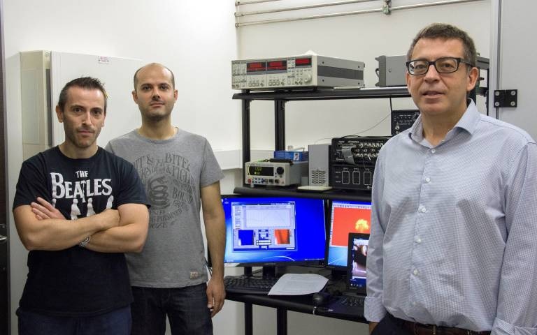
Scientists from Valencia’s Polytechnic University suggest a new design for antennas that are placed within chips, which comprise all the advantages of silicon photonics and plasmonics.
 (Image credit: Ruvid)
Scientists of the Polytechnic University of Valencia (UPV), from the Nanophotonic Technology Centre (NTC), have built new silicon nanoantennas for immediate use in communication and data processing for the next generation of reconfigurable photonic chips. This type of configurations paves the way towards the development of new tiny nanobiosensors and to the design of future networks and systems based on quantum optics. The work of the UPV scientists has been reported in the ACS Photonics journal.
The research carried out by the NTC-UPV team integrate for the first time the advantages of dielectric wireless applications (for the creation of reconfigurable networks, producing biosensors or beams) and the advantages of plasmonics (based on the use of metallic devices and interconnections for the rapid conversion of data or light engineering at nanoscale levels). This makes way for a new generation of ultra-integrated hybrid networks, which is the key contribution of the study.
We experimentally proved the first wireless dielectric-plasmonic connection thanks to a new type of dielectric nanoantenna that overcomes the limitations that plasmonics had until now, opening the door to new hybrid configurations. The results we have obtained have a direct implication in the design of reconfigurable communication networks inside the chip, in the development of ultra-fast optic devices, and in the practical implementation of ultra-compact biosensors.
Javier Martí, Head of NTC, UPV
He adds, “Thanks to plasmonic structures, this also opens the door to the creation of interfaces with future quantum systems.”
More efficient
As Sergio Lechago, scientist at the NTC and study’s co-author explains, plasmonic devices have facilitated the development of critical applications in fields such as spectroscopy, near-field and sensing optic microscopy because of their exceptional capability of controlling light on a nano level.
Within the communications combined in the chip, plasmonics facilitates the development of ultra-compact and economical devices (detectors, modulators, or sources) that can work at very high operation speeds using low amounts of energy.
The natural way of interconnecting these devices in the optic chip is by using metallic nanoguides. However, guiding light through these devices leads to very high propagation losses and entails certain restrictions regarding reconfigurability.
Carlos García Meca, Study Co-Author, NTC-UPV
He continued, “The use of plasmonic nanoantennas has been proposed to replace and improve the performance of guided metallic interconnections, but these antennas have low directivity and high losses which hinder their use in many practical applications.”
In this work, we overcame all these limitations by introducing a new dielectric nanoantenna design that acts as an efficient interface for plasmonic systems. This makes it possible to combine the benefits of plasmonics with those of silicon photonics, which can lead to more efficient, fast and reconfigurable chips.
Carlos García Meca, Study Co-Author, NTC-UPV
This innovation that took place in the laboratories of the Centre of Nanophotonic Technology of the UPV could also be utilized in fields such as biochemical or agri-food sectors, owing to the role that these hybrid systems can work as sensors with numerous purposes, allowing the interaction of light with nanoscopic inorganic and organic structures.
Source: http://ruvid.org

